Download PDF by clicking here
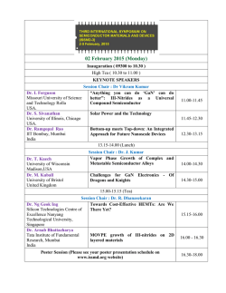
INAUGURATION - KEYNOTE SPEAKER
“Anything you can do ‘GaN’ can do better”:
III-Nitrides as a Universal Compound Semiconductor
Dr. Ian Ferguson, Fellow of IEEE, IOP and SPIE
Vice Provost and Dean of Engineering and Computing
Missouri University of Science and Technology
305 McNutt Hall, 1400 N. Bishop, Rolla,
MO 65409, USA
Dr. S. Sivanathan
Distinguished Professor of Physics, Director - Microphysics Laboratory
Department of Physics, University of Illinois at Chicago
845 W. Taylor St. MC 273, Room 2360 SES, Chicago IL 60607, USA
Title : Solar power and the technology
INTERNATIONAL PLENARY SPEAKERS
Dr. Thomas F. Kuech
National Academy of Engineering
Milton J. and A. Maude Shoemaker Chair of Chemical Engineering
UW-Foundation Chair Beckwith-Bascom Professor
University of Wisconsin – Madison, Department of Chemical and Biological Engineering
1415 Engineering Dr., Madison, WI 53711. USA
Title : Vapor Phase Growth of Complex and Metastable Semiconductor Alloys
Dr. Michel Pons
Directeur Science et Ingénierie des Matériaux et Procédés
SIMaP (Phelma Campus), UMR 5266 Grenoble INP, UJF, CNRS
1130 rue la Piscine, BP 75, 38402 Saint Martin D’Heres, FRANCE
Title : Functional properties and microstructure of AlN thin films and coatings
grown by CVD
Dr. Mohammed Henini
Professor of Applied Physics
International Postgraduate Recruitment&International Postgraduate Admissions Tutor
Nottingham Nanotechnology and Nanoscience Centre (NNNC)
School of Physics & Astronomy, University of Nottingham, Nottingham NG7 2RD, UK
Title : Development of Advanced Semiconductor Materials and Devices For Next
Generation Photovoltaics: Opportunities And Challenges
Dr. R. Muralidharan
Solid State Physics Laboratory
Lucknow Road, Delhi-110 054, INDIA
Title : Advances in GaN
Dr. V. Ramgopal Rao
Department of Electrical Engineering IIT Bombay,
Powai, Mumbai 400 076, India.
Title : Bottom-up meets Top-down: An Integrated Approach for Future Nanoscale
Devices
Dr. Ng Geok Ing,
Associate Professor, Director, Silicon Technologies Centre of Excellence
Nanyang Technological University, Research TechnoPlaza, 8th Storey, 50 Nanyang
Drive, Singapore 637553
Title : Towards Cost-Effective HEMTs: Are We There Yet?
Dr. Gen Sazaki
Laboratory for Phase Transition Dynamics of Ice
The Institute of Low Temperature Science, Hokkaido University,
N19-W8, Kita-ku, Sapporo 060-0819, JAPAN
Title : Direct visualization of surface melting processes: an example found on ice
crystal surfaces
Dr. Harri Lipsanen
Professor, Head of Department
Department of Micro- and Nanosciences, Micronova
Aalto University, P.O. Box 13500, FI-00076 Aalto, FINLAND
Title : III-V semiconductor nanowires for nanotechnology applications
INTERNATIONAL INVITED SPEAKERS
Dr. M. Kuball
Center for Device Thermography and Reliability (CDTR)
HH Wills Physics Laboratory, University of Bristol, United Kingdom.
Title : Challenges for GaN Electronics - Of Dragons and Knights
Dr. Shin Yokoyama
Associate Director, Research Institute for Nanodevice and Bio Systems
Hiroshima University, Japan
1-4-2 Kagamiyama, HIgashihirorshima 739-8527, Japan
Title: Si Ring Resonator and Photonic Crystal Resonator Biosensors
Prof Tae Won Kang
Quantum-functional Semiconductor Research Center and Department of Physics,
Dongguk University, 3-26, Pildong, Chungku, Seoul 100-715, KOREA
Title : Study on Properties and Applications of II-VI Nanostructures
Dr. John V Kennedy,
Principal Scientist, Environment ad Materials Division,
National Isotope Centre, GNS Science, 30 Gracefield Road, P O Box 31312,
Lower Hutt, 5010, New Zealand.
Title : Electronic, magneto transport and magnetic properties of Gadolinium
doped zinc oxide
Dr. S. Suresh
1CNRS, UMI 2958 Georgia Tech - CNRS, 57070 Metz,France
Title : Nanoselective area growth of III-nitrides for next generation devices.
Dr. L. Lazzarini
IMEM- CNR
Parma, ITALY
Title : Phase change GeSbTe based nanowires for data storage devices
Dr. Hoe Tan
Department of Electronic Materials Engineering
Research School of Physics and Engineering
Australian National University, Canberra, ACT0200, Australia
Title : Semiconductor nanowires for optoelectronic device applications
Dr. Alexander Crisci,
Institut polytechnique de Grenoble (Grenoble INP) - Phelma
Bâtiment Recherche Phelma / SIMaP / Bureau 116
1130 rue de la Piscine, 38 402 Saint Martin d'Hères, FRANCE
Title: Contribution of Electron Probe Microanalysis
characterisation scheme of thin layers
(EPMA)
to
the
Dr. Eric Faulques
Directeur de Recherche CNRS
UMR6502 Université de Nantes, Institut des Matériaux Jean Rouxel
2 rue de la Houssinière, F-44322 Nantes, FRANCE
Title: Studies of crystalline nanowires grown inside carbon nanotubes
Dr. Jesbains Kaur
Universiti Teknologi Malaysia (UTM),(University of Technology Malaysia)
Jalan Semarak 54100 Kuala Lumpur, Malaysia.
Title : Dependence of microstructures in MOVPE AlN on annealing temperature
of Sapphire substrate
INDIAN INVITED SPEAKERS
Dr. Vinay Gupta
Department of Physics and Astrophysics
University of Delhi, New Delhi
Title : Development of multifunctional materials for electronic devices
Dr. Arnab Bhattacharya
Dept. of Condensed Matter Physics and Materials Science
Tata Institute of Fundamental Research, Mumbai
Title: MOVPE growth of III-nitrides on 2D layered materials
Dr Anirban Bhattacharyya
Institute of Radiophysics and Electronics, University of Calcutta
92 Acharya Prafulla Chandra Road, Kolkata
Prof Anand P. Pathak ,FNASc, C Phys, F Inst P
School of Physics, University of Hyderabad,Central University P O, Hyderabad
Title: Ion Beam Studies of Semiconductor Nanostructures
Dr. R. Jeyakumar
Physics of Energy Harvesting Divisio,National Physical Laboratory, New Delhi
Title: Fabrication of c-Si solar cells using spin-on dopants
Dr. K. Jeganathan
Centre for Nanoscience & Nanotechnology,School of Physics, Bharathidasan
University, Tiruchirappalli
Title: Lattice matched and strained growth of InAlN/GaN heterostructure
Dr. Govind,
Physics of Energy Harvesting, National Physical Laboratory, New Delhi
Title: High quality GaN films grown on different substrates by molecular beam
epiatxy
Dr. Rajendra Singh
Department of Physics&Nanocale Research Facility Indian Institute of Technology
Delhi, Hauz Khas, New Delhi
Title: Fabrication and Characterization of GaN nanopillars for Applications in
Nanoscale Devices
Dr. S.K. Srivastava, Scientist, Silicon Solar Cells Group
Physics of Energy Harvesting, National Physical Laboratory, New Delhi
Title: Silicon nanowire arrays: A potential approach for efficient silicon solar cells
Dr. Rajesh K. Sharma
Solid State Physics Laboratory
Lucknow Road, Delhi
Title:Magneto-transport characterization of 2DEG in AlGaN/GaN HEMT structures
Dr. Souvik Mahapatra
Department of Electrical Engineering, IIT Bombay, Mumbai
Title: Macroscopic and Stochastic Aspects of Negative Bias Temperature
Instability in CMOS Devices and Circuits
Dr. Srinivasan Raghavan,
CeNSE, IISc, Bangalore
Title: Controlling Growth of Graphene and MoS2
Dr. Nandita Dasgupta
IIT , Chennai
Title: III-Nitride MIS-HEMTs –Two approaches to reduce Gate Leakage
Dr. K. Baskar
Crystal Growth Centre, Anna University, Chennai
Title:AlInGaN/AlN/GaN heterostructures grown by MOCVD
Dr. J. Kumar
Crystal Growth Centre, Anna University, Chennai
Title: On Dilute Magnetic Semiconductor related issues in GaN
Dr. R. THANGAVEL
Department of Applied Physics,Indian School of Mines, Dhanbad.
Title: Investigations on Zinc Oxide
© Copyright 2026
