
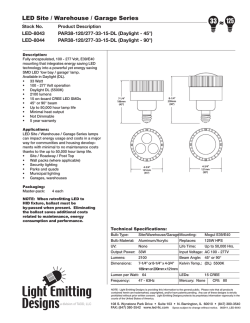
EE152 Final Presentation
DC-Link Input Exploration
Harry Johnson
Motivation:
General Specs:
●
●
●
●
●
SiC low-side FET
SiC high-side diode
1Mhz Switching Frequency
Output cap appropriately sized.
Average input current control loop.
Low-Side FET: Cree C2M0280120D
● 280mR RDSon
High-Side Diode: Cree C4D05120A
● Output current is actually rather low
● Optimize Qrr
MATLAB:
● Simple and quick to run sanity check
● Only models cycle-by-cycle, not control
inside cycle
● Results used earlier
LTSpice Overview:
● Models circuit behavior within cycle
● Runs for a single 120Hz cycle
● Exported setpoints from MATLAB to CSV, imported as
PWL files for current sources.
● Rest of Littlebox (main buck, DC-link output buck)
modeled as current sources where necessary.
● SiC devices: manufacturer-supplied models
LTSpice Schematic:
Main Buck Emulator
450V + 10R
DC-Link Input
Current Setpoint
Package
Inductance
Total Current setpoint: 5A
w/ soft start
DC-Link
Capacitor
Discharge
Current
Per-120Hz cycle plots.
Turn-On
Turn-Off
Calculated Results:
●
●
●
●
●
Averaged over the entire charge cycle
Power In: 1.3195KW
Power Out (into cap): 1.2888 KW
Switching Power Loss: 30.7 Watts
Eff: 97.6% (only including switching loss)
Areas for Future Work
● Model capacitor ESR appropriately for
mega-cap array (not modelled at all for
purposes of this simulation)
● Inductor losses: DCR relatively easy to
model but I suspect primary losses will be in
core.
● Actually build the darn thing!
Bonus: Megaderp moment
Late-night calculations:
● Automatic power calculation in LTspice (alt-click) on
Cree NMOS model.
● 500W !?
● Worked for a long time trying to optimize package, gate
drive, etc.
● Turns out I’m being autotrolled by the thermal
modelling, which is represented by voltage and current
sources.


© Copyright 2026