Datasheets
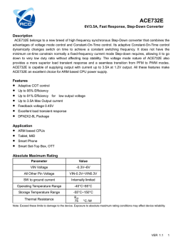
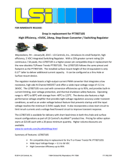
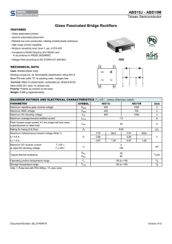
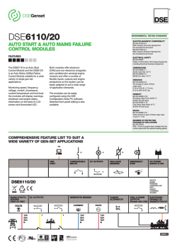
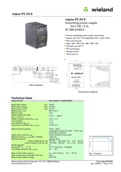
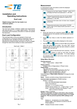
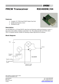
MIC33263/4 4MHz, 2A Buck Regulator with Integrated Inductor and HyperLight Load® General Description Features The MIC33263/4 is a highly-efficient synchronous buck regulator with an integrated inductor which provides the optimal trade-off between footprint and efficiency. The MIC33263/4 operates at 4MHz switching frequency and provides up to 2A output current. In addition, the 100% ® duty cycle and HyperLight Load (HLL) mode-of-operation delivers very-high efficiency at light loads and ultra-fast transient response which makes the MIC33263/4 perfectly suited for any space-constrained application and great alternative for low dropout regulators. An additional benefit of this proprietary architecture is very low output ripple voltage throughout the entire load range with the use of small output capacitors. • • • • • • The MIC33263/4 provides small compact total solution size of 4.6mm × 7mm with very few tiny external components. At higher loads, the MIC33263/4 provides a constant switching frequency around 4MHz while achieving peak efficiencies up to 93%. It also includes under-voltage lockout to ensure proper operation under power-sag conditions, internal soft-start to reduce inrush current, foldback current limit, power good (PG) indicator, and thermal shutdown. The MIC33263/4 is available in a 20-pin 2.5mm × 3.0mm × 1.9mm QFN package with an operating junction temperature range from –40°C to +125°C. Datasheets and support documentation are available on Micrel’s website at: www.micrel.com. • • • • • • • • • • Integrated MOSFETs, inductor 100% duty cycle 4MHz PWM operation in continuous mode 2A output current Low output voltage ripple 85% typical efficiency at 1mA and up to 93% peak efficiency Ultra-fast transient response Advanced copper lead frame design provides superior thermal performance Thermal-shutdown and current-limit protection Low-radiated emission (EMI) per EN55022, class B Adjustable output voltage 0.7V to 5V Configurable soft-start with pre-bias start-up capability Auto discharge of 180Ω (MIC33264 only) Low profile 2.5mm × 3.0mm × 1.9mm QFN packages 0.1µA shutdown current 33µA quiescent current Applications • • • • • • 5V point-of-load (POL) Low voltage distributed power systems Space-constrained applications Portable devices SSD storage systems Digital cameras Typical Application Efficiency vs. Output Current 100 90 EFFICENCY (%) 80 70 VOUT = 2.5V 60 VOUT = 1.8V VOUT = 1.2V 50 40 30 20 VIN = 3.3V 10 0 10 100 1000 OUTPUT CURRENT (mA) HyperLight Load is a registered trademark of Micrel, Inc. Micrel Inc. • 2180 Fortune Drive • San Jose, CA 95131 • USA • tel +1 (408) 944-0800 • fax + 1 (408) 474-1000 • http://www.micrel.com January 28, 2015 Revision 2.1 Micrel, Inc. MIC33263/4 Ordering Information Part Number Package (1, 2) Output Voltage Auto Discharge Junction Temperature Range MIC33263YGK ADJ No –40°C to +125°C 20-Pin 2.5mm × 3mm QFN MIC33264YGK ADJ Yes –40°C to +125°C 20-Pin 2.5mm × 3mm QFN Note: 1. QFN is a GREEN, RoHS-compliant package. Mold compound is Halogen Free. 2. Pb-free. Lead finish is matte tin. Pin Configuration 2.5mm × 3mm QFN (GK) (Top View) Pin Description Pin Number Pin Name 1, 20 PVIN Power Input Voltage: Connect a capacitor to PGND to decouple the noise. 2, 8, 9 PGND Power Ground. 3, 4, 5, 6, 7 SW 10, 11, 12, 13 VOUT Inductor Output. Connect a capacitor to PGND to filter the switcher output voltage. 14 AGND Analog Ground: Connect to central ground point where all high current paths meet (CIN, COUT, PGND) for best operation. 15 AVIN Analog Input Voltage: Connect a capacitor to ground to decouple the noise. 16 SS Soft-Start: Place a capacitor from SS pin to ground to program the soft-start time 17 PG Power Good: Open Drain output for the power good indicator. Place a resistor between this pin and a voltage source to detect a power good condition. 18 FB Feedback: Connect a resistor divider from the output to ground to set the output voltage. 19 EN Enable (Input): Logic high enables operation of the regulator. Logic low will shut down the device. Do not leave floating. January 28, 2015 Pin Function Switch (Output): Internal power MOSFET output switches. Disable pull down 180 Ohms (MIC33264 only). 2 Revision 2.1 Micrel, Inc. MIC33263/4 Absolute Maximum Ratings(3) Operating Ratings(4) Supply Voltage (VIN = VAVIN = VPVIN) .................. −0.3V to 6V Power Good Voltage (VPG) ................................ −0.3V to 6V Output Switch Voltage (VSW) ............................. −0.3V to 6V Enable Input Voltage (VEN) .. ..............................−0.3V to VIN Junction Temperature (TJ) ....................................... +150°C Storage Temperature Range (TS) ............. −65°C to +150°C Lead Temperature (soldering, 10s) ............................ 260°C (5) ESD Rating ................................................. ESD Sensitive Supply Voltage (VIN = VAVIN = VPVIN) ................. 2.7V to 5.5V Enable Input Voltage (VEN) .. ……………………….0V to VIN Feedback Voltage (VFB) ...................................... 0.7V to VIN Junction Temperature Range (TJ).. ….−40°C ≤ TJ ≤ +125°C Thermal Resistance 20-Pin 2.5mm × 3mm QFN (θJA) ........................ 50°C/W Electrical Characteristics(6) TA = 25°C; VIN = VEN = 3.6V; COUT = 22µF unless otherwise specified. Bold values indicate −40°C ≤ TJ ≤ +125°C, unless otherwise specified. Parameter Condition Min. 2.7 Supply Voltage Range Undervoltage Lockout Threshold Typ. 2.40 Turn-On Undervoltage Lockout Hysteresis 2.53 Max. Units 5.5 V 2.65 V 75 mV Quiescent Current IOUT = 0mA , VSNS > 1.2 × VOUT Nominal 33 85 µA Shutdown Current VEN = 0V; VIN = 5.5V 0.1 2 µA +2.5 % 0.717 V Output Voltage Accuracy VIN = 3.6V if VOUTNOM < 2.5V, ILOAD = 20mA VIN = 5.5V if VOUTNOM ≥ 2.5V, ILOAD = 20mA Feedback Regulation Voltage Current Limit VSNS = 0.9 × VOUTNOM Output Voltage Line Regulation VIN = 3.6V to 5.5V, ILOAD = 20mA Output Voltage Load Regulation PWM Switch On-Resistance −2.5 0.682 0.7 2.5 3.3 A 0.3 %/V 0.3 % 0.13 Ω 4 MHz 1000 µs 2.2 µA 20mA ≤ ILOAD ≤ 1A, VIN = 3.6V 20mA ≤ ILOAD ≤ 1A, VIN = 5.5V ISW = 100mA PMOS ISW = −100mA NMOS Switching Frequency IOUT = 120mA Soft-Start (SS) Time VOUT = 90%, CSS = 1nF Soft-Start (SS) Current VSS = 0V Power Good (PG) Threshold (Rising) % of VNOM 85 90 95 % Notes: 3. Exceeding the absolute maximum ratings may damage the device. 4. The device is not guaranteed to function outside its operating ratings. 5. Devices are ESD sensitive. Handling precautions are recommended. Human body model, 1.5kΩ in series with 100pF. 6. Specification for packaged product only January 28, 2015 3 Revision 2.1 Micrel, Inc. MIC33263/4 Electrical Characteristics(6) (Continued) TA = 25°C; VIN = VEN = 3.6V; COUT = 22µF unless otherwise specified. Bold values indicate −40°C ≤ TJ ≤ +125°C, unless otherwise specified. Parameter Condition Min. Power Good Threshold Hysteresis Typ. Max. 7 Power Good Pull-Down VSNS = 90% VNOMINAL, IPG = 1mA Enable Threshold Turn-On 0.5 Units % 60 200 mV 0.8 1.2 V Enable Hysteresis 70 Enable Input Current 0.1 Overtemperature Shutdown 160 °C Overtemperature Shutdown Hysteresis 20 °C 180 Ω SW Pull-Down Resistance (MIC33264 only) January 28, 2015 VEN = 0V 4 mV 2 µA Revision 2.1 Micrel, Inc. MIC33263/4 Typical Characteristics Efficiency vs. Output Current 100 90 90 80 80 VOUT = 1.2V VOUT = 1.8V VOUT = 2.5V 60 50 40 30 VOUT = 2.5V 70 VOUT = 1.8V 60 RISE TIME (µs) 70 VOUT = 3.3V VOUT = 1.2V 50 40 10000 1000 100 30 20 VIN = 3.3V 10 10 100 10 VIN = 5V 20 0 VIN = 3.6V 1 10 1000 10 100 100 1000 OUTPUT CURRENT (mA) OUTPUT CURRENT(mA) Current Limit vs. Input Voltage Quiscent Current vs. Input Voltage 1000 10000 100000 1000000 CSS (pF) Quiscent Current vs. Temperature 45 4 35 40 3.8 30 35 3.6 25 3.4 3.2 IQ (µA) 30 IQ (µA) 25 20 15 10 2.8 VOUT = 2.4V VOUT = 2V NO LOAD 3.5 4 4.5 5 5.5 0 2.5 3 3.5 4 4.5 VIN (V) Line Regulation (Light Loads) Line Regulation (High Loads) 2.006 OUTPUT VOLTAGE (V) 2.005 2.004 50mA 2.002 2.001 2 150mA 1.999 5 3 3.5 4 4.5 INPUT VOLTAGE (V) January 28, 2015 5 5.5 -20 0 20 40 60 80 100 120 Output Voltage vs. Output Current (DCM) 2.018 2.08 2.016 2.07 2.06 2.014 2.012 2A 2.01 2.008 2.006 500mA 2.004 2.002 2.05 2.04 2.03 2.02 2.01 2 1.99 1.98 300mA 2 VIN = 3.6V 1.97 1.998 2.5 -40 5.5 TEMPERATURE (°C) INPUT VOLTAGE (V) 2.003 VIN = 3.6V VOUT =1.75V 5 0 3 15 5 2.6 2.5 20 10 3 OUTPUT VOLTAGE (V) CURRENT LIMIT (A) 1000000 100000 EFFICIENCY (%) EFFICENCY (%) 100 OUTPUT VOLTAGE (V) VOUT Rise Time vs. CSS Efficiency vs. Output Current 1.96 2.5 3 3.5 4 4.5 INPUT VOLTAGE (V) 5 5 5.5 0 20 40 60 80 100 120 140 160 180 200 OUTPUT CURRENT (mA) Revision 2.1 Micrel, Inc. MIC33263/4 Typical Characteristics (Continued) Output Voltage vs. Output Current (CCM) PG Threshold vs. Input Voltage Output Voltage vs. Temperature 2.05 1.85 92 1.83 91 PG THRESHOLD (% OF VREF) 2.06 OUTPUT VOLTAGE (V) OUTPUT VOLTAGE (V) 2.04 2.03 2.02 2.01 2 1.99 1.98 1.97 1.96 VIN = 3.6V 1.81 1.79 1.77 1.75 1.73 1.71 1.69 1.67 1.95 VIN = 3.6V 1.65 1.94 -40 200 400 600 800 1000 1200 1400 1600 1800 2000 -20 0 20 40 60 80 100 90 PG RISING 89 88 87 86 85 84 PG FALLING 83 82 120 2.5 3 3.5 TEMPERATURE (°C) OUTPUT CURRENT (mA) UVLO Threshold vs. Temperature 4.5 5 5.5 Enable Thresholds vs. Input Voltage Enable Threshold vs. Temperature 2.6 4 VIN (V) 0.9 1 0.8 0.95 ENABLE THRESHOLD (V) 2.56 2.54 2.52 UVLO OFF 2.5 2.48 2.46 0.7 0.6 0.5 0.4 0.3 0.2 0.1 2.44 0 -40 -20 0 20 40 60 80 100 120 -40 -20 TEMPERATURE (°C) FEEDBACK VOLTAGE (V) SW FREQUENCY (KHz) 0 20 40 60 80 100 VIN = 3.6V 1000 VIN = 5V 100 10 VOUT = 2V 1 1000 January 28, 2015 CFF = 1nF TCASE = 25°C 2.5 3 10000 3.5 4 4.5 5 5.5 INPUT VOLTAGE (V) Shutdown Current vs. Temperature 0.2 0.715 0.71 0.705 0.7 0.695 VIN = 3.6V VOUT = 1.75V IOUT = 30mA 0.69 0.685 0.18 0.16 0.14 0.12 0.1 0.08 0.06 0.04 VIN = 3.6V 0.02 0 0.68 100 0.7 0.6 120 0.72 10 0.8 0.75 Feedback Voltage vs. Temperature 10000 OUTPUT CURRENT (mA) 0.85 TEMPERATURE (°C) Switching Frequency vs. Output Current 1 0.9 0.65 SHUTDOWN CURRENT (µA) UVLO THRESHOLD (V) 2.58 ENABLE VOLTAGE (V) UVLO ON -40 -20 0 40 20 60 80 TEMPERATURE (°C) 6 100 120 -40 -20 0 20 40 60 80 100 120 TEMPERATURE (°C) Revision 2.1 Micrel, Inc. MIC33263/4 Functional Characteristics January 28, 2015 7 Revision 2.1 Micrel, Inc. MIC33263/4 Functional Characteristics (Continued) January 28, 2015 8 Revision 2.1 Micrel, Inc. MIC33263/4 Functional Characteristics (Continued) January 28, 2015 9 Revision 2.1 Micrel, Inc. MIC33263/4 Functional Diagram Figure 1. Simplified MIC33263/4 Functional Block Diagram − Adjustable Output Voltage January 28, 2015 10 Revision 2.1 Micrel, Inc. MIC33263/4 Functional Description PVIN The input supply (PVIN) provides power to the internal MOSFETs for the switch-mode regulator. The PVIN operating input voltage range of 2.7V to 5.5V so an input capacitor, with a minimum voltage rating of 6.3V, is recommended. Due to the high switching speed, a minimum 2.2µF bypass capacitor placed close to PVIN and the power ground (PGND) pin is required. Refer to the PCB Layout Recommendations section for details. AGND The analog ground (AGND) is the ground path biasing and control circuitry. The current loop signal ground should be separate from the power (PGND) loop. Refer to the PCB Recommendations section for details. PGND The power ground pin is the ground path for the high current in PWM mode. The current loop for the power ground should be as small as possible and separate from the analog ground (AGND) loop as applicable. Refer to the PCB Layout Recommendations section for details. AVIN Analog VIN (AVIN) provides power to the internal control and analog supply circuitry. AVIN must be tied to PVIN. Careful layout should be considered to ensure that any high-frequency switching noise caused by PVIN is reduced before reaching AVIN. A 1µF capacitor as close to AVIN as possible is recommended. Refer to the PCB Layout Recommendations section for details. PG The power good (PG) pin is an open drain output which indicates logic high when the output voltage is typically above 90% of its steady state voltage. A pull-up resistor of more than 5kΩ should be connected from PG to VOUT. EN/Shutdown A logic high signal on the enable pin activates the output voltage of the device. A logic low signal on the enable pin deactivates the output and reduces supply current to 0.1µA. When disabled the MIC33264 switches an internal load of 180Ω on the regulators switch node to discharge the output. The MIC33263/4 features external soft-start circuitry adjusted by the soft-start (SS) pin that reduces in-rush current and prevents the output voltage from overshooting at start up. Do not leave the EN pin floating. SS The soft-start (SS) pin is used to control the output voltage ramp-up time. Setting CSS to 1nF sets the startup time to the recommended minimum of approximately 575µs. The start-up time can be determined by Equation 1: TSS = 250 × 10 3 × ln(10 ) × C SS SW The switch (SW) connects to the controller end of integrated inductor. The other end of the inductor is connected to the VOUT pin. Due to the high-speed switching on this pin, the switch node should be not be connected. Eq. 1 The action of the soft-start capacitor is to control the rise time of the internal reference voltage between 0% and 100% of its nominal steady-state value. FB This is the control input for programming the output voltage. A resistor divider network is connected to this pin from the output and is compared to the internal 0.7V reference within the regulation loop. VOUT The output pin (VOUT) connects to the output of integrated inductor. The output capacitor should be connected from this pin to PGND as close to the module as possible. The MIC33263/4 is rated for an output current of up to 2A. A 22µF capacitor is recommended for best performance. Refer to the PCB Layout Recommendations section for details. January 28, 2015 for the for the ground Layout 11 Revision 2.1 Micrel, Inc. MIC33263/4 The output voltage can be programmed between 0.7V and 5V using Equation 2: R1 VOUT = VREF × 1 + R2 Eq. 2 where: R1 is the top resistor, R2 is the bottom resistor. Table 1. Example Feedback Resistor Values VOUT R1 R2 1.2V 215k 301k 1.5V 301k 261k 1.8V 340k 215k 2.5V 274k 107k 3.3V 383k 102k 3.6V 422k 102k 5V 634k 102k January 28, 2015 12 Revision 2.1 Micrel, Inc. MIC33263/4 Application Information Efficiency Considerations Efficiency is defined as the amount of useful output power, divided by the amount of power supplied, as shown in Equation 3: The MIC33263/4 is a high-performance DC/DC stepdown regulator offering a small solution size of 4.6mm × 7mm. Supporting an output current up to 2A inside a tiny 3mm × 2.5mm QFN package, the MIC33263/4 requires very few external components while meeting today’s miniature portable electronic device needs. Using the ® (HLL) switching scheme, the HyperLight Load MIC33263/4 is able to maintain high efficiency throughout the entire load range while providing ultra-fast load transient response. The following sections provide additional device application information. V ×I Efficiency % = OUT OUT V ×I IN IN Eq. 3 Maintaining high efficiency serves two purposes. It reduces power dissipation in the power supply, reducing the need for heat sinks and thermal design considerations and it reduces consumption of current for battery-powered applications. Reduced current draw from a battery increases the device’s operating time and is critical in hand held devices. Input Capacitor A 2.2µF ceramic capacitor or greater should be placed close to the PVIN pin and PGND pin for bypassing. A TDK C1608X5R0J475M, size 0603, 4.7µF ceramic capacitor is recommended based upon performance, size, and cost. A X5R or X7R temperature rating is recommended for the input capacitor. Y5V temperature rating capacitors, aside from losing most of their capacitance over temperature, can also become resistive at high frequencies. This reduces their ability to filter out high-frequency noise. There are two types of losses in switching converters; DC losses and switching losses. DC losses are simply the 2 power dissipation of I R. Power is dissipated in the high side switch during the on cycle. Power loss is equal to the high side MOSFET RDSON multiplied by the switch current squared. During the off cycle, the low side N-channel MOSFET conducts, also dissipating power. Device operating current also reduces efficiency. The product of the quiescent (operating) current and the supply voltage represents another DC loss. The current required driving the gates on and off at a constant 4MHz frequency and the switching transitions make up the switching losses. Output Capacitor The MIC33263/4 is designed for use with a 22µF or greater ceramic output capacitor. Increasing the output capacitance will lower output ripple and improve load transient response but could also increase solution size or cost. A low equivalent series resistance (ESR) ceramic output capacitor such as the TDK C1608X5R1A226M080AC, size 0603, 22µF ceramic capacitor is recommended based upon performance, size and cost. Both the X7R or X5R temperature rating capacitors are recommended. The Y5V and Z5U temperature rating capacitors are not recommended due to their wide variation in capacitance over temperature and increased resistance at high frequencies. Figure 2 shows an efficiency curve. From no load to 100mA, efficiency losses are dominated by quiescent current losses, gate drive and transition losses. By using the HLL mode, the MIC33263/4 is able to maintain high efficiency at low output currents. Efficiency vs. Output Current Compensation The MIC33263/4 is designed to be stable with a 22µF ceramic (X5R) output capacitor. An external feedback capacitor of 15pF to 68pF is required for optimum regulation performance. 100 90 EFFICIENCY (%) 80 100% Duty Cycle Low Dropout Operation The MIC33263/4 enters 100% duty cycle when the input voltage gets close to the nominal output voltage, in this case the high-side MOSFET switch is turned on 100% for one or more cycles. By decreasing the input voltage further the high-side MOSFET switch turns on completely. In this case the small difference between VIN and VOUT is determined by RDSON and DCR of the inductor. This is extremely useful in battery-powered applications to accomplish longest operation time. January 28, 2015 × 100 VOUT = 2.5V 70 VOUT = 1.8V 60 VOUT = 3.3V VOUT = 1.2V 50 40 30 VIN = 5V 20 10 10 100 1000 OUTPUT CURRENT(mA) Figure 2. Efficiency under Load 13 Revision 2.1 Micrel, Inc. MIC33263/4 Emission Characteristic of MIC33263/4 Over 100mA, efficiency loss is dominated by MOSFET RDSON and inductor losses. Higher input supply voltages will increase the gate-to-source threshold on the internal MOSFETs, thereby reducing the internal RDSON. This improves efficiency by reducing DC losses in the device. The MIC33263/4 integrates switching components in a single package, so the MIC33263/4 has reduced emission compared to standard buck regulator with external MOSFETs and inductors. The radiated EMI scans for MIC33263/4 are shown in the Functional Characteristics. The limit on the graph is per EN55022 class B standard. ® HyperLight Load Mode (HLL) MIC33263/4 uses a minimum on and off time proprietary control loop (PCL) patented by Micrel called HyperLight ® Load (HLL). When the output voltage falls below the regulation threshold, the error comparator begins a switching cycle that turns the PMOS on and keeps it on for the duration of the minimum-on-time. This increases the output voltage. If the output voltage is over the regulation threshold, then the error comparator turns the PMOS off for a minimum-off-time until the output drops below the threshold. The NMOS acts as an ideal rectifier that conducts when the PMOS is off. Using a NMOS switch instead of a diode allows for lower voltage drop across the switching device when it is on. The asynchronous switching combination between the PMOS and the NMOS allows the control loop to work in discontinuous mode for light load operations. In discontinuous mode, the MIC33263/4 works in pulse frequency modulation (PFM) to regulate the output. As the output current increases, the off-time decreases, thus provides more energy to the output. This switching scheme improves the efficiency of MIC33263/4 during light load currents by only switching when it is needed. As the load current increases, the MIC33263/4 goes into continuous conduction mode (CCM) and switches at a frequency centered at 4MHz. As shown in Figure 3, as the output current increases, the switching frequency also increases until the MIC33263/4 goes from HLL mode to PWM mode at approximately 120mA. The MIC33263/4 will switch at a relatively constant frequency around 4MHz once the output current is over 220mA. Switching Frequency vs. Output Current SW FREQUENCY (KHz) 10000 VIN = 3.6V 1000 VIN = 5V 100 10 VOUT = 2V 1 1 10 100 1000 10000 OUTPUT CURRENT (mA) Figure 3. SW Frequency vs. Output January 28, 2015 14 Revision 2.1 Micrel, Inc. MIC33263/4 Typical Application Schematic Bill of Materials Item C1 Part Number Manufacturer Description Qty. (7) C1608X5R1A475K080AC TDK GRM188R60J475KE19D Murata (8) 4.7µF, 10V, X5R, Size 0603 1 C2 C1608X5R1A105K TDK 1µF, 10V, X5R, Size 0603 1 C3 C1005C0G1H102J050BA TDK 1nF, 50V, 0402 1 C1005C0G1H150J050BA TDK GRM1555C1H150JZ01D Murata 15pF, 50V, 0402 1 C1608X5R1A226M080AC TDK 22µF,10V, X5R, Size 0603 1 301kΩ, 1%, 1/16W, Size 0402 1 C4 C5 (9) R1 CRCW0402301KFKEA R2 CRCW0402158K0FKEA Vishay 158kΩ, 1%, 1/16W, Size 0402 1 R3, R4 CRCW0402100KFKEA Vishay 100kΩ, 1%, 1/16W, Size 0402 1 R5 CRCW040249R9FKED Vishay 49.9Ω, 1%, 1/16W, Size 0402 1 4MHz, 2A Buck Regulator with Integrated Inductor and HyperLight Load 1 U1 MIC33263YGK MIC33264YGK Vishay (10) Micrel, Inc. Notes: 7. TDK: www.tdk.com. 8. Murata: www.murata.com. 9. Vishay: www.vishay.com. 10. Micrel, Inc.: www.micrel.com. January 28, 2015 15 Revision 2.1 Micrel, Inc. MIC33263/4 PCB Layout Recommendations Top Layer Bottom Layer January 28, 2015 16 Revision 2.1 Micrel, Inc. MIC33263/4 Package Information and Recommended Landing Pattern(11) 20-Pin 2.5mm × 3mm QFN (GK) Note: 11. Package information is correct as of the publication date. For updates and most current information, go to www.micrel.com. January 28, 2015 17 Revision 2.1 Micrel, Inc. MIC33263/4 MICREL, INC. 2180 FORTUNE DRIVE SAN JOSE, CA 95131 USA TEL +1 (408) 944-0800 FAX +1 (408) 474-1000 WEB http://www.micrel.com Micrel, Inc. is a leading global manufacturer of IC solutions for the worldwide high-performance linear and power, LAN, and timing & communications markets. The Company’s products include advanced mixed-signal, analog & power semiconductors; high-performance communication, clock management, MEMs-based clock oscillators & crystal-less clock generators, Ethernet switches, and physical layer transceiver ICs. Company customers include leading manufacturers of enterprise, consumer, industrial, mobile, telecommunications, automotive, and computer products. Corporation headquarters and state-of-the-art wafer fabrication facilities are located in San Jose, CA, with regional sales and support offices and advanced technology design centers situated throughout the Americas, Europe, and Asia. Additionally, the Company maintains an extensive network of distributors and reps worldwide. Micrel makes no representations or warranties with respect to the accuracy or completeness of the information furnished in this datasheet. This information is not intended as a warranty and Micrel does not assume responsibility for its use. Micrel reserves the right to change circuitry, specifications and descriptions at any time without notice. No license, whether express, implied, arising by estoppel or otherwise, to any intellectual property rights is granted by this document. Except as provided in Micrel’s terms and conditions of sale for such products, Micrel assumes no liability whatsoever, and Micrel disclaims any express or implied warranty relating to the sale and/or use of Micrel products including liability or warranties relating to fitness for a particular purpose, merchantability, or infringement of any patent, copyright, or other intellectual property right. Micrel Products are not designed or authorized for use as components in life support appliances, devices or systems where malfunction of a product can reasonably be expected to result in personal injury. Life support devices or systems are devices or systems that (a) are intended for surgical implant into the body or (b) support or sustain life, and whose failure to perform can be reasonably expected to result in a significant injury to the user. A Purchaser’s use or sale of Micrel Products for use in life support appliances, devices or systems is a Purchaser’s own risk and Purchaser agrees to fully indemnify Micrel for any damages resulting from such use or sale. © 2014 Micrel, Incorporated. January 28, 2015 18 Revision 2.1
© Copyright 2026
