
High-energy x-ray reflectivity of buried interfaces created by wafer
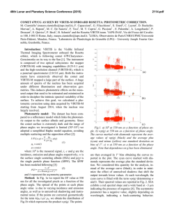
PHYSICAL REVIEW B, VOLUME 63, 125408 High-energy x-ray reflectivity of buried interfaces created by wafer bonding F. Rieutord,1 J. Eymery,1 F. Fournel,1 D. Buttard,1 R. Oeser,1 O. Plantevin,1 H. Moriceau,2 and B. Aspar2 1 CEA-De´partement de Recherche Fondamentale Sur la Matie`re Condense´e, 17 rue des Martyrs, 38054 Grenoble Cedex 9, France 2 CEA-LETI, De´partement de Microtechnologies, 17 Rue des Martyrs 38054 Grenoble Cedex 9, France 共Received 11 April 2000; revised manuscript received 19 October 2000; published 13 March 2001兲 The bonding interfaces separating two silicon wafers assembled for making a silicon-on-insulator system are studied using high-resolution high-energy x-ray reflectivity. The evolution of the bond structure upon annealing is investigated, in situ. These data directly exhibit water removal and oxide layer structural changes, throughout the temperature sequence. DOI: 10.1103/PhysRevB.63.125408 PACS number共s兲: 61.10.Kw, 68.35.Ct, 68.55.Jk, 68.35.⫺p Wafer bonding is an important technique for joining materials in microelectronics and micromechanics. It relies on the fact that two surfaces will stick together when brought into contact if they are sufficiently clean, mirror polished, flat, and dust free. Applications include silicon-on-insulator substrates fabrication, which is of large use in microelectronics for low-voltage or high-temperature device manufacturing.1 The large experience gained in the design of artificial bonds between two materials also allows other applications to be envisioned for this interface fabrication technique. However, we are still lacking methods to characterize these interfaces buried between thick materials. Standard transmission x-ray diffraction techniques can be used,2 but interface-specific techniques are scarce due to the fact that most radiation used in surface studies 共e.g., low- and highenergy electrons, light or conventional x rays兲 are unable to cross millimeters of solid material since they interact too strongly with the embedding bulk material. Scanning probe techniques 关scanning tunnel microscopy 共AFM兲兴 can at best be used on cross sections of the material. The method we shall use here meets the seemingly contradictory requirements of a large bulk penetration and a high interface sensitivity. It is based on the use of high-energy x-rays under grazing incidence conditions. Due to their high energy, the x-rays can cross several millimeters of bulk material without a too large absorption while the use of shallow angles allows an increased sensitivity to the interface. We shall concentrate in this paper on high-energy x-ray reflectivity 共HEXRR兲 but off-specular scattering and grazing incidence scattering have been performed in the same conditions, with the same interest, and data will be published in forthcoming papers. To our knowledge, this is the first study of a deeply buried solid interface using this technique. With this technique, we could obtain detailed structural information on the bonding interface, giving access to the physical process occurring at this interface. The geometry of the experiment is shown in Fig. 1. The samples used were made by bonding a wafer covered by a thin native oxide layer to a wafer on which 400 or 500 Å of thermal oxide were grown. The x rays enter the sample from one edge, are reflected by the interfaces, and exit on the other edge. The length of the sample should be of the order of, or smaller than the attenuation length of the material. However the use of high-energy x rays causes an angular compression 0163-1829/2001/63共12兲/125408共5兲/$15.00 of the reflectivity features and imposes a higher collimation of the beam. In these experiments requiring the crossing of silicon or SiO2 material, we used an x-rays energy of 27 keV and a sample length L of 4 mm, which is two times the attenuation length for silicon at this energy. The beam size at sample position was 50 m so that at very small angles the beam was larger than the interface cross section h 关h ⫽L sin , being the incident angle 共see Fig. 1兲兴. A correction for this geometrical factor was applied. It should be noted that in all the experiments, the distance between the interface and the external surfaces is 0.5 mm 共wafer thickness兲 so that, in the angular range used, the beam never hits the outer surfaces. This is actually the main asset of the technique: as for standard optical reflectivity, reflection comes from index changes 共i.e., for x rays, electron density changes兲. As the radiation does not reach the outer interfaces, the reflection signal is merely due to the change of density in the interfacial zone and the signal is free from any contribution of the strong density gradients at the air 共vacuum兲-material interfaces. In this respect, a zero background technique as a perfect interface between similar material would just produce no signal: the interfacial zone under study behaves like a free-standing film.3 It should be noted that the incidence of the beam to the sample edge is close to 90°, so that reflection or refraction effects at the entrance or the exit of the beam are negligible. Another point that is worth noting is that this geometry allows reflectivity at both negative and positive incidences to be performed. FIG. 1. Sketch of the HEXRR experiment: the beam enters from the side of one of the wafers, is reflected by the interfacial area density gradients, and exits on the other side. Absorption through the system is taken into account via normalization to the transmitted beam. 63 125408-1 ©2001 The American Physical Society F. RIEUTORD ET AL. PHYSICAL REVIEW B 63 125408 to express the reflectivity as a function of these parameters is based on the assumption that each interface in the profile ‘‘sees’’ the same incident wave and reflects with a phase depending only on its position along z. This is a kinematical approximation and, in this approximation, the reflectivity is the Fourier transform of the index gradient profile R共 q 兲⫽ 64 4 4q 4 冏冕 ⫹⬁ ⫺⬁ 冏 2 dn 共 z 兲 exp共 iqz 兲 dz , dz 共1兲 where n is the refractive index, the wavelength, and q ⫽4 / sin is the wave-vector transfer in the geometry. The front factor in 1/q 4 corresponds to the reflection of a perfect diopter separating two media with a unity index change 共fresnel reflectivity兲. When this dependence is removed by considering q 4 R(q), this formula gives, for a slab delimited by two boundaries, a sinusoidal dependence with unity contrast: FIG. 2. Reflection curve of a buried silicon oxide film obtained by hydrophilic bonding of a native oxide and thermal oxide covered wafers. The solid line is a fit to data points using a simplest twoparameter box model (d⫽499 Å,⌬ ⫽⫺2.5%). Data at both positive and negative incidences are shown. The experiments were performed on the bending magnet beamline of the Collaborative Research Group on Interfaces 共CRG-IF兲 at the European Synchrotron Radiation Facility. This beamline gives a monochromatic beam of the order of 1010 ph/s in a 0.3⫻0.3 mm focal spot with a convergence of 1 mrad⫻0.1 mrad. The reflectivity was taken using standard /2 scans. Alignment was checked periodically by performing rocking scans 共 alone兲. At very small angle the detector is very close to the transmitted beam and some background is produced. The background 共off-specular scattering兲 was measured by performing detector scans and keeping the sample at ⫽0 and subtracted off the /2 signal. The level of this background is negligible as soon as angles not too close to the direct beam are considered. Normalization was performed using the transmitted beam, which includes both incident beam intensity and transmission coefficient. We shall first describe the results obtained on a system of a thin silicon oxide film embedded between two 0.5 mm silicon wafers. This system was obtained by bonding two silicon wafers, one covered with native oxide 共thickness ⬃7–8 Å兲 and one covered with thermally grown oxide 共thickness ⬃500 Å兲. High-temperature (T⬎1000 °C) annealing was then performed, ex-situ, during 3 h. Reflectivity obtained for both negative and positive small angles is shown in Fig. 2. As it can be seen, many well-contrasted fringes are observed, a fact which is not surprising as the two boundary media are identical and very flat. In the angular range shown, the data can be fit using a simple two-parameter model. The thickness is measured from the fringe spacing and the fringe intensity is related to the refractive index gradient at both interfaces. For x rays, this is just proportional to the electron-density gradients: far from any absorption edge 共our case兲, the refractive index is related to the electron density el by n⫽1⫺ 2 /(2 )r 0 el , where r 0 is the classical electron radius. The simplest model q 4 R 共 q 兲 ⫽ 共 4 r 0 兲 2 兩 ⌬ 关 ⫺1⫹exp共 iqd 兲兴 兩 2 . 共2兲 The fit to the data yields 兩 ⌬n 兩 ⫽1.910⫺8 ( 兩 ⌬ 兩 ⫽0.02 Å ⫺3 ) corresponding to a density difference of 2.5% between silicon and silicon oxide. The thickness measured on this sample is 499 Å, very close to the value of 500 Å expected from the growth kinetics of the thermal oxide. Telling if the density of the oxide is 2.5% higher or lower than that of silicon is actually not obvious as both values could be physically relevant for this system, which has experienced a high-temperature annealing. Equations 共1兲 or 共2兲 would give a similar result in both cases. However, at very small angles, kinematical approximation breaks down and the actual values of the reflectivities for the two density profiles are very different. They can be calculated using another formalism based on the optical theory of x rays. In this model, one discretizes the profile into a stack of thin slabs of constant index. The reflectivity is then recursively computed from the contribution of each slab.4,5 As this optical model takes into account the full set of transmitted and reflected waves at each interface, it corresponds to the dynamical treatment of x-ray diffraction and is correct whatever the angle. If silica were 2.5% denser than silicon, the index change at the silicon-silicon oxide interface would be negative so that total ‘‘external reflection’’ would be expected below an angle given by Snell Descartes law c⫽ 冑2 兩 ⌬n 兩 . Although located at very small angles and close to the direct transmitted beam, reflection in this angular range is measurable when background subtraction is performed. Comparison of experimental data to the curves calculated using a dynamical theory 共optical兲 model clearly indicates that the situation is that of a positive index gradient, with no total external reflection. The mass density of the silicon oxide film is thus 2.27 g/cm3 共electron density 0.683 Å⫺3兲, i.e., less dense than silicon ( Si⫽2.33 g/cm3). This value is to be compared to the density of tridymite, a variety of silica that forms in a temperature range consistent with the annealing temperature. From the data of Fig. 2 alone, it is not possible to determine a value for the interfacial roughness l r (l r ⫽0 was used in the fits without any incidence on the results兲. A maximum value 125408-2 HIGH-ENERGY X-RAY REFLECTIVITY OF BURIED . . . PHYSICAL REVIEW B 63 125408 FIG. 3. Electron-density model used to fit the temperaturedependent measurements. The density dip at the bonding interface is modeled by a Gaussian well of width and depth ⌬ dip . can be given (l r ⬍2 Å) and more details could be obtained only if data on a larger q range were considered. One of the advantages of the technique of HEXRR is that it can be performed in-situ during the annealing that is used to increase the bond strength. We have performed this study using a Meca2000 UHV-compatible furnace installed in a custom-made vacuum chamber equipped with beryllium windows 共vacuum was of the order of 10⫺6 mbar during experiment兲. The sample considered was similar to the previous one, i.e., Si/SiO2 共native 7–8 Å兲 bound to a SiO2 共thermal, 400 Å兲/Si wafer. The reflection curve at ambient temperature shows two main features. First, the reflection level is much higher than for the annealed system, typically by two orders of magnitude 共see Fig. 4兲. As the intensity reflected by an interface is proportional to the magnitude of the electron-density gradient at this interface 关see Eq. 共1兲 or 共2兲兴, this indicates that large density gradients are now present in the system. As the silicon-silicon oxide interfaces have only weak density changes, these large index gradients are due to the lack of electrons at the bonding interface. Second, fringes are still visible but their contrast C 关defined as C⫽(I max⫺Imin)/(Imax⫹Imin)兴 is low. This again is due to the fact that these fringes are due to interference between the large density gradients at the interface and the small ones at the Si/SiO2 interfaces. The interference between the native oxide-silicon interface and the bond interface is not visible: as these two interfaces are close to each other, they would give in q space a long period fringe that is not separable from the contribution due to the shape of the interfacial electron density gap. To model quantitatively the reflection data, we used, as shown in Fig. 3, an electron-density profile where the dip at the bonding interface is represented by a ‘‘Gaussian well’’ of width and depth ⌬ dip• (z)⫽⫺⌬ dip exp(⫺z2/2 2 ). With the notation of Fig. 3, the Fourier transform 共1兲 becomes FIG. 4. 共a兲 Normalized q 4 R(q) reflection curves of a wafer bonding assembly as a function of annealing temperature. Very large intensity variations are seen due to the evolution of the interfacial bond gap structure. 共b兲 enlarged part (scale⫻100) of T ⫽900 °C, 1h00 data together with high-temperature annealed system 共squares兲 关i.e., data of Fig. 2, in q 4 R(q) representation兴. sion of Eq. 共3兲: When the density gap ⌬ dip at the bonding interface is large, the terms including it dominate those involving the small SiO2 /Si density gradients (⌬ SiO2 /Si) and Eq. 共3兲 approximates under the form q 4 R 共 q 兲 / 共 4 r 0 兲 2 ⫽ 共 ⌬ dip 兲 2 2 q 2 exp共 ⫺q 2 2 兲 ⫹2 共 ⌬ dip 兲 ⌬ SiO2 /Siq 冑2 ⫻exp共 ⫺q 2 2 /2兲 sin共 qd th兲 . In this expression, the first term on the right-hand side reproduces the hump of the curves in the q 4 R(q) representation, while the second term is the interference term responsible for the fringes. This expression shows that the depth and width of the electron deficit at the bonding interface are readily determined from the maximum amplitude and width of the reflection curves: the q 4 R(q) signal displays a hump, which is the Fourier transform of the dip profile. As the bond gap fills in, this hump disappears. Using the second term in Eq. 共4兲, one can work out an expression for the fringes contrast: q 4 R 共 q 兲 ⫽ 共 4 r 0 兲 2 兩 ⌬ SiO2 /Si兵 ⫺1⫹exp关 iq 共 d nat⫹d th兲兴 其 C⫽ ⫺⌬ dipiq 冑2 exp共 ⫺q 2 2 /2兲 exp共 iqd nat兲 兩 2 , 共3兲 where d nat and d th are the thicknesses of the native and thermal oxide layers. This expression shows directly how to interpret the experimental data of Fig. 4. The influence of the different parameters can be best understood using an expan- 共4兲 2⌬ SiO2 /Si ⌬ dip 冑2 q exp共 ⫺q 2 2 兲 ⫽ 2⌬ SiO2 /Si 冑具 I 共 q 兲 典 , 共5兲 where 具 I(q) 典 is the reflection intensity averaged over a fringe period. From this expression one can readily obtain the silicon oxide silicon density gradient. Data were collected at ambient, 200, 800, and 900 °C 共see Fig. 4兲. Due to the kinetics at high temperature only a limited part of q range could be scanned. Curves 900-1 and 900-2 125408-3 F. RIEUTORD ET AL. PHYSICAL REVIEW B 63 125408 TABLE I. Fit parameters used to describe the reflectivity data of Fig. 4 using the model of Eq. 共3兲. Temperature Ambient 200 °C 800 °C 900 °C t⫽0 900 °C t⫽1h00 Thermal oxide thickness d th 共Å兲 Surface area S of the dip 共Å⫺2兲 Width of the dip 共Å兲 Depth of the dip ⌬ dip 共Å⫺3兲 Thermal oxide density SiO2 共Å⫺3兲 388 387 395 398 404a 2.6 2.9 2.5 1.0 0.15 4.4 4.1 5.5 6 7 0.23 0.28 0.18 0.07 0.01 0.683 0.683 0.662 0.662 0.662 a This value includes the native oxide thickness as the bond gap is very weak for this last set of data. refers to two sets of data taken at 900 °C with a one-hour time interval. The parameters obtained from fit of Eq. 共3兲 to the data are shown in Table I. At ambient temperature, the surface area S of the density ‘‘well,’’ which is directly related to both the level of reflection and the width of the hump, is 2.6 Å⫺2. This parameter is actually the first data that can be extracted from the reflection data 共e.g., from low q data兲, as it is the first moment of the density distribution at the interface.6 The width parameter of the dip, which is the second moment of the electrondensity distribution, is 4.2 Å. This corresponds to a full width at half maximum of w 1/2⫽ 冑(2 Ln2)⫽10 Å. The depth of electron-density deficit is obtained from the height of the hump 关first term in Eq. 共4兲 for q ⫽1兴 or through ⌬ dip⫽S/ 冑(2 )/ . The electron density in the well ( el ⫽ SiO2⫺⌬ dip) can be determined from this data. The value found is consistent with the idea that the bond gap may actually be filled with water, assuming water keeps its bulk electron density. Our data indicate that 3–4 monolayers of water are present at the interface and this should be viewed as a maximum since part of the gap may just be empty, thus reducing the amount of water necessary to achieve the measured electron deficit. This observation is consistent with the values observed using infrared absorption spectroscopy.7–9 We believe this number of layers is intimately linked to the presence of bound water layers at the surfaces of hydrophilic wafers and the physics of dewetting involved during the propagation of the bond wave. When temperature is raised to 200 °C, the reflected intensity is higher than at ambient temperature 共by 50%兲 which means that the deficit of electron density has increased 共by 25%兲. From the measure of both the dip surface area change and the width change, one can estimate the amount of water that has left the interface to one monolayer, with a remaining quantity of 2–3 monolayers. This partial removal of water can be associated to the observed increase in surface energy observed in this temperature range 共typically from 0.15 J/m2 to 1.0 J/m2兲 due to formation of siloxane bonds. At 800 °C, the reflected intensity starts to decrease and comes back below the ambient temperature data. The overall value of the electron-density deficit at the interface is still important, but the width starts to increase, indicating that the gap gets shallower. Note that the range of our data is smaller as we limited the duration of the experiment to a few minutes to limit the evolution of the material during the annealing. Indeed, this temperature of 800 °C is known to correspond to the beginning of SiO2 chemical modification. The interesting point is that the fringe spacing indicates that the thickness of the thermal oxide has increased by 7–8 Å. Correlatively, the fringe amplitudes indicate that the density gradient between silicon and silicon oxide has increased. The fit to the data indicate a decrease of the density of silicon oxide by another 2% to a value of SiO2⫽2.20 g/cm3 共0.662 Å⫺3兲, which is the standard for amorphous silica. The thermal expansion of the oxide being low 共⬍0.5 Å兲, this increase in thickness correlated to a reduction in density is certainly due to some phase transformation taking place in the thermal oxide under heating. The kinetic evolution of the bond gap is most visible on the data taken at 900 °C. On the first curve taken 2 hours after the 800 °C data, the gap has reduced by a factor of 4 in surface area. One hour later, it has almost disappeared and the data show unity contrast fringes as observed on the hightemperature annealed system described in the first part of the paper 共Fig. 2兲. This evolution is in-line with the possibility for the oxide to flow at these high temperatures, thus allowing a fill up of the gap between the two oxide surfaces. The thickness deduced from fringe spacing on the last curve has now increased by another 9 Å compared to the 800 °C value. This increase is the result of two factors. First, the incorporation of the native oxide thickness. The fringe spacing no longer yields the distance between the dip and the thermal oxide-silicon interface but the distance between the two Si/SiO2 interfaces. This distance includes the thickness of the native oxide 关i.e., approximation 共4兲 is no longer valid in this case兴. Second, the gap closing. Assuming no material is lost, the closure of the gap induces a reduction of the distance between the two Si/SiO2 interfaces by about 4 Å, obtained from the ratio of the surface area of the electron density gap 共2.5 Å⫺2兲 to the silicon oxide electron density 共0.66 Å⫺3兲. These data means that the thickness of the native oxide was close to 13 Å. It should be noted that as long as the electrondensity gap at the bonding interface is large, the thickness of the native oxide could not be extracted from the data and this parameter value was kept fixed to a value of 8 Å. Finally it is interesting to compare the last data of the annealing sequence to the previously described fully annealed system, studied ex-situ 共Fig. 4b兲. Apart from the difference in fringe period due to the different oxide layer thickness used in the ex-situ sample 共500 Å instead of 400 Å兲, the fringe amplitude and contrast are similar. This shows that the 125408-4 HIGH-ENERGY X-RAY REFLECTIVITY OF BURIED . . . PHYSICAL REVIEW B 63 125408 electron density dip was almost filled up after 1 h at this temperature. Only the slight increase in intensities of fringe minima and maxima for the 900 °C sample is indicative of a remaining small electron deficit at the bonding interface, a deficit that is no longer measurable on the ex-situ annealed sample. High-energy x-ray reflectivity is one of the few techniques available to characterize bonding interfaces buried between thick materials. It allows a direct determination of the electron-density profile of the interface with an angstrom resolution. The technique allows a direct control of molecu- 1 Q.-Y. Tong and U. Go¨sele, Semiconductor Wafer Bonding: Science and Technology 共Wiley, New York, 1999兲. 2 M. Nielsen et al., Surf. Sci. 442, L989 共1999兲; S. Weichel et al., Appl. Phys. Lett. 76, 70 共2000兲. 3 E. A. L. Mol et al., Phys. Rev. Lett. 79, 3439 共1997兲; J.-J. Benattar et al., Prog. Colloid Polym. Sci. 105, 113 共1997兲. 4 M. Born and E. Wolf, Principles of Optics 共Pergamon Press, New lar reorganization taking place during the formation of the bond interface. It readily gives the closing temperature of the gap and allows one to follow the associated growth and density changes of the oxide layers. We have seen here some examples on the most classical bonding procedures used industrially 共room-temperature bonding in air, followed by annealing兲 but the method is suited to test the influence of various parameters on the bonding 共e.g., chemical and physical surface treatment, surface roughness, ion implantation兲. Other systems and bonds between other materials 共e.g., metallic films兲 can also be studied by this technique. York, 1980兲. L. G. Parratt, Phys. Rev. 95, 359 共1954兲. 6 F. Rieutord et al., Physica B 221, 1 共1996兲. 7 R. Stengl et al., Jpn. J. Appl. Phys. 28, 1735 共1989兲. 8 D. Feijoo´ et al., Appl. Phys. Lett. 65, 2548 共1994兲. 9 A. Milekhin et al., J. Vac. Sci. Technol. B 17, 1733 共1999兲. 5 125408-5

© Copyright 2026