
Raman microscopy mapping for the purity
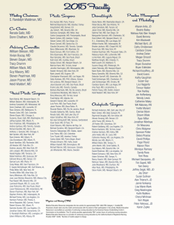
Nano Research Nano Res DOI 10.1007/s12274-015-0725-y 1 Raman microscopy mapping for the purity assessment of chirality enriched carbon nanotube networks in thin film transistors Zhao Li ( ), Jianfu Ding, Paul Finnie, Jacques Lefebvre, Fuyong Cheng, Christopher T. Kingston, Patrick R. L. Malenfant ( ) Nano Res., Just Accepted Manuscript • DOI 10.1007/s12274-015-0725-y http://www.thenanorese arch.com on January 28, 2015 © Tsinghua University Press 2015 Just Accepted This is a “Just Accepted” manuscript, which has been examined by the peer-review process and has been accepted for publication. A “Just Accepted” manuscript is published online shortly after its acceptance, which is prior to technical editing and formatting and author proofing. Tsinghua University Press (TUP) provides “Just Accepted” as an optional and free service which allows authors to make their results available to the research community as soon as possible after acceptance. After a manuscript has been technically edited and formatted, it will be removed from the “Just Accepted” Web site and published as an ASAP article. Please note that technical editing may introduce minor changes to the manuscript text and/or graphics which may affect the content, and all legal disclaimers that apply to the journal pertain. In no event shall TUP be held responsible for errors or consequences arising from the use of any information contained in these “Just Accepted” manuscripts. To cite this manuscript please use its Digital Object Identifier (DOI®), which is identical for all formats of publication. TABLE OF CONTENTS (TOC) Raman microscopy mapping for the purity assessment of chirality enriched carbon nanotube networks in thin film transistors SWCNT network Purity and density Via Raman Mapping -2 -3 Zhao Li,* Jianfu Ding, Paul Finnie, Jacques Lefebvre, Fuyong Cheng, Christopher T. Kingston, Patrick R. L. Log (ISD) -4 -5 -6 2.5 um -7 5 um -8 Malenfant* Security and -10 -5 0 5 10 VG (V) Disruptive Technologies Portfolio, National Research Council Canada, 1200 Montreal Road, Ottawa, Ontario, K1A 0R6, Canada Raman microscopy mapping can be a powerful characterization tool to quantify residual metallic carbon nanotubes in high density networks of enriched semiconducting single walled carbon nanotubes. www.nrc.ca Nano Research DOI (automatically inserted by the publisher) Research Article Raman microscopy mapping for the purity assessment of chirality enriched carbon nanotube networks in thin film transistors Zhao Li ( ), Jianfu Ding, Paul Finnie, Jacques Lefebvre, Fuyong Cheng, Christopher T. Kingston, Patrick R. L. Malenfant ( ) Received: day month year ABSTRACT Revised: day month year With recent improvements in carbon nanotube separation methods, the accurate determination of residual metallic carbon nanotubes in a purified nanotube sample is important, particularly for those interested in using semi-conducting single walled carbon nanotubes (SWCNT) in electronic device applications such as thin film transistors (TFT). This work demonstrates that Raman microscopy mapping is a powerful characterization tool to quantify residual metallic carbon nanotubes present in highly enriched semiconducting nanotube networks. Raman mapping correlates well with absorption spectroscopy, yet provides greater differentiation in purity. Electrical data from TFTs with channel lengths of 2.5 and 5 microns demonstrate the utility of the method in a device context. By comparing samples with nominal purities of 99.0% and 99.8%, a clear differentiation can be made when evaluating the current on/off ratio as a function of channel length and as such, the Raman mapping method provides a means to guide device fabrication by correlating SWCNT network density and purity with TFT channel scaling. Accepted: day month year (automatically inserted by the publisher) © Tsinghua University Press and Springer-Verlag Berlin Heidelberg 2014 KEYWORDS Raman spectroscopy, Carbon nanotubes, Thin film transistors, Microscopy mapping, purity assessment. Address correspondence to Zhao Li, [email protected]; Patrick R. L. Malenfant, [email protected] 2 Nano Res. As prepared SWCNT raw materials contain bundles of nanotubes with a 2:1 semiconducting (sc-) to metallic (m-) ratio and other impurities such as catalyst and amorphous carbon [1-3]. For electrical devices, these raw materials must be debundled, purified and enriched [4-11]. It has been demonstrated that for network thin film transistors (TFT), the m-tube content should be less than 2% [3]. For more demanding applications, such as high frequency logic circuits and display backplanes, the m-tube content should be less than a few ppm given the need for high mobility and current on/off ratios [12]. In recent years, multiple efforts have led to significant progress in solution based enrichment techniques, with sc-SWCNT purity in excess of 99% routinely achieved. This leap, however, has now started to reveal the limits of common characterization methods and other tools are required to provide accurate purity assessment [13,14]. Typically, the purity of enriched sc-SWCNT is estimated from the UV absorption spectrum by comparing the peak areas associated with the m- or sc- species [12, 15-17]. This method works well for samples when these peaks are well defined and background absorption is not dominant. However, as the sc-purity increases, the features associated with m-tube absorption will gradually disappear and the precise subtraction of the background absorption will dramatically influence the calculated results and introduce uncertainty [18]. As an alternative, we have previously used a different purity metric, denoted φ, which is based on the ratio of the sc-peak area over the total absorption background from the metallic (M11) and semiconducting (S 22) absorption bands [16]. While we presume φ correlates well with purity for highly pure samples, it does not provide a quantitative assessment. Furthermore, a solution sample is not necessarily representative of the deposited networks on a solid substrate, such as a transistor channel, where selective adsorption may occur [19]. There is currently a need for a quick and reliable method to quantitatively characterize a SWCNT network for its residual m-SWCNT content in fabricated TFTs in order to better understand device performance as a function of SWCNT network density and purity. Methods for the measurement of m-SWCNT content can be divided into bulk sample techniques and counting-based techniques. Counting-based techniques more accurately enumerate m- and sc-nanotubes and typically rely on their electrical and/or optical performance [20-29]. Although these methods give relatively accurate results, they involve tedious fabrication processes and costly instruments. Furthermore, most of these methods are only applicable to sparse SWCNT networks (<1 tube/µm2), which is significantly below the typical tube network density used in TFTs (10-40 tubes/µ m2). Raman spectroscopy is commonly used to characterize SWCNT ensembles [30-36] and can also be used for individual nanotubes due to its high sensitivity and chirality selective resonance with laser irradiation wavelength [37-39]. Raman spectroscopy not only discriminates m- and sc- tubes, but also enables the assignment of specific chiralities to individual tubes [40-42]. Raman spectroscopy, especially in the G band region, can be very sensitive to metallic SWCNT contamination, and it is useful for the purity assessment of highly pure SWCNT samples [36]. Herein, we will demonstrate that Raman microscopy mapping is an efficient and effective characterization method for large area, high density, high sc purity SWCNT networks in TFTs [43-45]. SWCNT networks were formed on Si/SiO2 substrates by soaking the later in toluene dispersions [16]. Networks formed by soaking are random in terms of position and orientation of nanotubes. This type of network produces TFTs with good performance (high current density and current on/off ratio) and are accessible using scalable fabrication processes. Although the Raman mapping method presented here will be proven with random nanotube networks, it should be equally applicable to aligned nanotubes. Raman microscopy was performed by raster scanning a defined area. While scanning we can monitor each spectrum and record the position of interest to determine tube type and the validity of the signal to eliminate false positives. Finally, a map or image can be built by selecting specific Raman peaks/bands. Figure 1 shows the Raman spectra and mapping images of the network under 514 nm laser excitation. According to the Kataura plot, a 514 nm laser is resonant mainly with sc-nanotubes for the range of tube diameters used here (~1.3 nm) [46-47]. | www.editorialmanager.com/nare/default.asp 3 Nano Res. The dark area at the top of the images is the evaporated TFT electrode. Figure 1(b) and 1(d) show the intensity mapping of the G + band from 1581 to 1602 cm-1 and RBM band from 140 to 208 cm -1, respectively (all Raman mapping images have been processed and raw data can be found in the ESM). These two maps show similar intensity patterns, confirming these two bands come from the resonance of tubes at the same position. Several representative spectra covering D and G bands extracted at the marked spots in Figure 1(b) are shown in Fig. 1(a), which are typical sc-tube Raman spectra [30-36]. Figure 1(c) shows the RBM bands of these spots and the peaks centered at 190 cm-1 correspond to 1.30 nm diameter (10, 9) sc-tubes, agreeing well with the result from PLE mapping [16]. Figure 1 Raman spectra and maps for excitation at 514 nm. (a) G band spectra; (b) G+ map obtained from integrated intensities in the 1581-1602 cm-1 range; (c) RBM band spectra and (d) RBM map obtained from integrated intensities in the 140-208 cm-1 range. Circles in (b) and (d) highlight positions from which spectra were taken in (a) and (c). Scanned area was 16×16 μm2 and scale bar is 2 µm. The concentration of the SWCNT solution was 7.6 mg/L and the networks were prepared by submerging the substrate for 10 min in the SWCNT solution. The purpose of this work is to quantitatively assess the minority m-SWCNT species buried in the sc-SWCNT network. Given the diameter distribution of the sample used here, 633 nm laser excitation matches well with the M11 absorption resonance. Figure 2(a) compares the Raman spectra in the 1200 to 1700 cm-1 region under 514 and 633 nm laser excitation spatially averaged over the whole scanned area. The spectrum from 633 nm excitation has a clear metallic signature with a broad G - band (Breit-Wigner-Fano lineshape), in contrast with the sharper G- seen at 514 nm [30-36, 49-50]. Since the sample is highly sc-enriched, the off resonance contribution from sc-tubes at 633 nm is non-negligible, especially for the spatially averaged spectra as in Figure 2(a). However, individual spectra generated from 1 µ m2 defined pixels will be dominated by m-SWCNTs resonant under 633 nm excitation considering their much higher scattering cross-section. Figure 2 633 nm Raman spectra and maps taken from the same area as in Fig. 1. (a) Spatially averaged Raman spectra covering the whole area (normalized to G+ band); (b) G+ and (d) G- map obtained from integrated intensities in the 1581-1602 and 1507-1547 cm-1 range; (c) G band spectra; (e) RBM band spectra and (f) RBM map obtained from integrated intensities in the 149-210 cm-1 range. Circles in (b), (d) and (f) highlight positions from which spectra were taken in (c) and (e). Scanned area was 16×16 μm2 and scale bar is 2 µm. www.theNanoResearch.com∣www.Springer.com/journal/12274 | Nano Research 4 Nano Res. The Raman intensity mapping of the G + band under 633 nm laser excitation in Fig. 2(b) shows different patterns compared to 514 nm laser excitation (Fig. 1(b)), meaning Raman signals originated from different tube species. Figure 2(d) shows the G- band intensity mapping covering 1507 to 1547 cm -1, where bright spots correspond only to m-SWCNTs in this area. By analyzing the raw spectra for each pixel, we found 21 locations in the scanned area having typical m-SWCNT G- band signals with the Raman spectra shown on Fig. 2(c). We count one metallic tube if the spectrum has a strong (signal visually well above noise floor; for a signal:noise ratio of approximately 3:1) and broad Gpeak at 1530-1560 cm-1. Variation in intensity from pixel to pixel can be related to tube chirality, length and its overlap with the laser spot [30-37]. For strong G- signals that extend over several contiguous pixels, the spectra were analyzed to determine if each spot contained one or more m-tubes. Given an average tube length of 1.2 μm and given that a 0.5 m raster increment was used to assess each pixel, if identical spectra were collected over multiple adjacent pixels, only a single m-tube was counted (it is statistically improbable that two metallic tubes are situated in adjacent pixels). Most of the RBM bands of these pixels (Fig. 2(e)) show only one peak, meaning no more than one diameter of m-SWCNT per pixel were found. In such cases, we assumed that only one nanotube was present at that location. Only one RBM band (green trace in Fig. 2(e)) displays two peaks at 170.8 and 185.0 cm-1, indicating two m-SWCNTs within that pixel. The diameter of these two m-SWCNTs are calculated to be 1.45 and 1.34 nm and they are assigned to (15, 6) or (16, 4) and (14, 5) respectively, considering their resonance with 633 nm irradiation [30-36]. In order to calculate the purity in the SWCNT networks, we use SEM charge contrast imaging to obtain an accurate measure of the nanotube network density of the same area (a 4 µ m 2 area was used to count tubes at high magnification). For the sample in Fig. 1-2, a density of 40 nanotubes/μm2 was measured, which amounts to 104 nanotubes for the 16×16 µ m2 area. (Fig. S1). As a result, the residual m-SWCNT content is estimated to be 0.2%. Note that this method may underestimate m-SWCNT content due to off resonance or no G - contribution from armchair SWCNT [51]. Armchair SWCNTs have unique Raman spectra and we did not observe any in our networks [51]. Statistically speaking, only 3 armchair tubes species would be expected given the diameter range of the enriched SC-SWCNTs we have isolated [(9,9); (10,10); (11,11)]. Assuming an even distribution of chiralities in the unsorted starting material, armchair tubes in our diameter regime would represent less than 10% of all metallic tubes, a negligible contribution to the underestimation. Figure 3 Calibration of G+ band intensity versus carbon nanotube coverage determined by SEM. The scanned area was 16×16 µm2. The intensity for both wavelengths was normalized for easy comparison. To expedite the method, a Raman mapping calibration curve that obviates the need for repeated SEM was established. Networks with tube densities ranging from 2 to 100 tubes/µm 2 were made using different SWCNT solution concentrations and analyzed by SEM (Fig. S2). Figure 3 shows the G+ peak intensity at 1591 cm-1 averaged over a 16×16 µ m2 area under 514 nm or 633 nm laser excitation vs SEM tube network density. Good linearity is found for network densities up to 40 tubes/µ m 2. We should emphasize that at higher tube coverage it becomes increasingly difficult to accurately count tubes using charge contrast SEM imaging as evidenced by the outlying data point observed in Figure 3 (~80 nanotubes/m2). As a result, it is possible to estimate both the tube network density and sc purity using exclusively Raman microscopy mapping (vide infra). | www.editorialmanager.com/nare/default.asp 5 Nano Res. 1000 1 (a) 800 SC1 Intensity Absorption (a.u.) 0.8 SC2 0.6 0.4 (b) SC1 600 SC2 400 200 0.2 0 400 800 1200 1600 2000 0 1200 1300 1400 1500 1600 1700 1800 Raman Shift (cm-1) Wavelength (nm) SC1, 633 nm (G-) (c) 25 1E+8 20 1E+6 On/off ratio Mobility SC2, 633 nm (G-) (f) 1E+7 (e) (cm2/Vs) (d) 1E+5 15 1E+4 10 1E+3 1E+2 5 SC2 SC1 SC1 SC1 0 2.5 5.0 2.5 5.0 Channel Length (µm) 1E+1 1E+0 SC1 SC2 2.5 5.0 2.5 5.0 Channel Length (µm) Figure 4 (a) UV absorption spectra of enriched sc-tube samples SC1 and SC2 in solution. (b) Raman spectra averaged from 20×20 µm2 area for networks prepared from SC1 and SC2 for excitation at 633 nm. (c) and (d) G- maps obtained from integrated intensities in the 1507-1547 cm-1 range for networks prepared from SC1 and SC2 respectively. (e) Mobility and (f) current on/off ratio of thin film transistors prepared from SC1 and SC2. The channel width is 2000 µm. Transfer curves can be found in Figure S3 in the ESM. The validity of the Raman mapping method for the sc-purity evaluation was further confirmed using two conjugated polymer enriched sc-SWCNT samples (SC1 and SC2). As shown in Fig. 4(a), the UV-vis absorption curve of SC2 (ɸ=0.40) has a much deeper valley centered at 630 nm than that from SC1 (ɸ=0.33), and the Raman spectrum of the SC2 network has a lower intensity of G- band at 1540 cm-1 (Fig. 4(b)). Although both data indicate higher m-SWCNT content in SC1, we only have qualitative information [5]. We then scanned an area 20×20 µ m2 using 633 nm laser excitation for each network and intensity mapping was done using a G- window spanning 1507 to 1547 cm-1 (Fig. 4(c) and 4(d)). We counted 135 and 20 m-SWCNT signals for SC1 and SC2 networks respectively. Using the calibration curve in Figure 3, the tube density of these two networks was calculated to be ~ 30 tubes/µ m2. As a result, the m-SWCNT content was estimated to be 1.0% and 0.2%, thus the sc-nanotube purity was estimated at 99.0% and 99.8% for SC1 and SC2, respectively. In order to assess the correlation between SC purity and channel length, samples SC1 and SC2 were further compared as the semiconducting channel material in thin film transistors. A SWCNT network was combined with a bottom gate, bottom contact device configuration with interdigitated S/D electrodes having a 2000 µ m channel width [16]. Devices were prepared under identical conditions with regards to solution concentration and TFT performance data are summarized in Fig. 4(e) and 4(d). At 5 µ m channel lengths the TFTs have very similar mobility values of 20±2 cm 2/Vs and excellent current on/off ratios, reaching as high as 1x10 7. However, devices with 2.5 µ m channel lengths clearly reveal the purity difference between SC1 and SC2 even though similar mobility values of 16±1 cm2/Vs were obtained. In a representative sampling of four devices, all four 2.5 µ m channel length TFTs from SC1 had on/off ratios < 1x10 4, with three devices < 1x10 3 while three TFTs from SC2 had on/off ratios > 1x10 6 and only one device had an on/off ratio between 10 3 and 10 4. The TFT data at 2.5 µm channel lengths agrees with the purity differentiation obtained by Raman mapping, further substantiating the ability of the method to discriminate between highly enriched sc-SWCNT samples. A statistical model was used to determine the probability of a percolation path to form (see ESM for calculations). For TFTs with a channel length of 2.5 m, we expect 1 metallic path every 290 μm for a network with 0.2% metallic tube content (SC2) or every 5 μm for 1% metallic tube content (SC1). Given that our channel width is 2000 m, a few short circuits, if any, are expected for the higher purity sample, while short circuits should be fairly abundant in the lower purity sample. Given that the on currents are of the order of several mA, and with several short circuits contributing current of the order of 1 μA in the off state, on-off ratios of the order of 10 3 are expected for the lower purity sample (SC1), consistent with our purity assessment. In summary, Raman mapping has been shown to be an efficient and effective method to quantitatively evaluate sc-purity and SWCNT network density directly in fabricated TFT devices. The accuracy of www.theNanoResearch.com∣www.Springer.com/journal/12274 | Nano Research 6 Nano Res. the method was further validated by sc-SWCNT network TFT device performance at short channel lengths. The advantage of using networks of SC-SWCNT over aligned tubes [52-55] for the active channel in TFTs is the favorable trade-off between targeted performance and ease of fabrication [56-58]. Such TFTs will find utility in low cost display driver and logic circuit elements fabricated using scalable deposition techniques such as dip-coating, ink-jet or gravure printing [59-66]. This work bridges the gap between separation methods that yield high purity sc-SWCNTs and available characterization tools for purity assessment thus providing a framework for device design that considers TFT channel scaling with SWCNT density and purity. Acknowledgements The authors would like to thank Jeff Fraser for SEM imaging. Electronic Supplementary Material: Supplementary material (Materials, SWCNT film preparation, TFT device fabrication and testing, resonance Raman spectra mapping method and representative SEM images) is available in the online version of this article at http://dx.doi.org/10.1007/s12274-***-****-* (automatically inserted by the publisher). References [1] Avouris, P. Molecular electronics with carbon nanotubes. Acc. Chem. Res. 2002, 35, 1026-1034. [2] De Volder, M. F. L.; Tawfick, S. H.; Baughman, R. H.; Hart, A. J. Carbon nanotubes: present and future commercial applications. Science 2013, 339, 535-539. Noorden, R. V. The trials of new carbon. Nature 2011, 469, 14-16. Zhang, H.; Wu, B.; Hu, W.; Liu, Y. Separation and/or selective enrichment of single-walled carbon nanotubes based on their electronic properties. Chem. Soc. Rev. 2011, 40, 1324-1336. [3] [4] [5] [6] [7] Wang, C.; Takei, K.; Takahashi, T.; Javey, A. Carbon nanotube electronics-moving forward. Chem. Soc. Rev. 2013, 42, 2592-2609. Lu, F.; Meziani, M. J.; Cao, L.; Sun, Y.-P. Separated metallic and semiconducting single-walled carbon nanotubes: opportunities in transparent electrodes and beyond. Langmuir 2011, 27, 4339-4350. Liu, Z.; Jiao, L.; Yao, Y.; Xian, X.; Zhang, J. Aligned, ultralong single-walled carbon nanotubes: from synthesis, sorting, to electronic devices. Adv. Mater. 2010, 22, 2285-2310. [8] Hu, L.; Hecht, D. S.; Grüner, G. Carbon Nanotube thin films: fabrication, properties, and applications. Chem. Rev. 2010, 110, 5790-5844. [9] Park, S.; Vosguerichian, M.; Bao, Z. A review of fabrication and applications of carbon nanotube film-based flexible electronics. Nanoscale 2013, 5, 1727-1752. [10] Rouhi, N.; Jain, D.; Burke, P. J. High-performance semiconducting nanotube inks: progress and prospects. ACS Nano 2011, 5, 8471-8487. [11] Sun, D.-M.; Liu, C.; Ren, W.-C.; Cheng, H.-M. A review of carbon nanotube- and graphene-based flexible thin-film transistors. Small 2013, 9, 1188-1205. [12] Mistry, K. S.; Larsen, B. A.; Blackburn, J. L. High-yield dispersions of large-diameter semiconducting single-walled carbon nanotubes with tunable narrow chirality distributions. ACS Nano 2013, 7, 2231-2239. [13] Itkis, M. E.; Perea, D. E.; Jung, R.; Niyogi, S.; Haddon, R. C. Comparison of analytical techniques for purity evaluation of single-walled carbon nanotubes. J. Am. Chem. Soc. 2005, 127, 3439-3448. [14] Itkis, M. E.; Perea, D. E.; Niyogi, S.; Rickard, S. M.; Hamon, M. A.; Hu, H.; Zhao, B.; Haddon, R. C. Purity evaluation of as-prepared single-walled carbon nanotube soot by use of solution-phase near-IR spectroscopy. Nano Lett. 2003, 3, 309-314. [15] Gomulya,W.; Costanzo,G. D.; Figueiredo de Carvalho,E. J.; Bisri, S. Z.; Derenskyi,V.; Fritsch,M.; Fröhlich, N.; Allard, S.; Gordiichuk ,P.; Herrmann, A.; Marrink, S. J.; Santos, M. C.; Scherf, U.; Loi, M. A. Semiconducting single-walled carbon nanotubes on demand by polymer wrapping. Adv. Mater. 2013, 25, 2948-2956. [16] Ding, J.; Li, Z.; Lefebvre, J.; Cheng, F.; Dubey, G.; Zou, S.; Finnie, P.; Hrdina, A.; Scoles, L.; Lopinski, G.; Kingston, C.; Simard, B.; Malenfant, P. R. L. Enrichment of large-diameter semiconducting SWCNTs by polyfluorene extraction for high network density thin film transistors. Nanoscale 2014, 6, 2328-2339. [17] Tange, M.; Okazaki, T.; Iijima, S. Selective extraction of large-diameter single-wall carbon nanotubes with specific chiral indices by Poly (9,9-dioctylfluorene-alt -benzothiadiazole). J. Am. Chem. Soc. 2011, 133, 11908-11911. [18] Naumov, A. V.; Ghosh, S.; Tsyboulski, D. A.; Bachilo, S. M. Weisman, R. B. Analyzing absorption backgrounds in single-walled carbon nanotube spectra. ACS Nano 2011, 5, 1639-1648. [19] LeMieux, M. C.; Roberts, M.; Barman, S.; Jin, Y. W.; Kim, J. M.; Bao, Z. Self-sorted, aligned nanotube networks for thin-film transistors. Science 2008, 321, 101-104. [20] Gao, M.; Zuo, J. M.; Twesten, R. D.; Petrov, I.; Nagahara, L. A.; Zhang, R. Structure determination of individual single-wall carbon nanotubes by nano area electron diffraction. Appl. Phys. Lett. 2003, 82, 2703-2705. [21] Qin, L. C.; Iijima, S.; Kataura, H.; Maniwa, Y.; Suzuki, S.; Achiba, Y. Helicity and packing of single-walled carbon nanotubes studied by electron nanodiffraction. Chem. Phys. Lett. 1997, 268, 101-106. [22] Wildöer, J. W. G.; Venema, L. C.; Rinzler, A. G.; Smalley, R. | www.editorialmanager.com/nare/default.asp 7 Nano Res. E.; Dekker, C. Electronic structure of atomically resolved carbon nanotubes. Nature 1998, 391, 59-62. A. G.; Pimenta, M. A.; Saito, R. Single nanotube Raman spectroscopy. Acc. Chem. Res. 2002, 35, 1070-1078. [23] Lu, W.; Xiong, Y.; Hassanien, A.; Zhao, W.; Zheng, M.; Chen, L. A Scanning probe microscopy based assay for single-walled carbon nanotube metallicity. Nano Lett. 2009, 9, 1668-1672. [38] Doorn, S. K.; Heller, D. A.; Barone, P. W.; Usrey, M. L.; Strano, M. S. Resonant Raman excitation profiles of individually dispersed single walled carbon nanotubes in solution. Appl. Phys. A 2004, 78, 1147-1155. [24] Vijayaraghavan, A. ; Blatt, S. ; Marquardt, C. ; Dehm, S.; Wahi R. Hennrich, F.; Krupke, R. Imaging electronic structure of carbon nanotubes by voltage-contrast scanning electron microscopy. Nano Res. 2008, 1, 321-332. [39] Hennrich, F.; Krupke, R.; Lebedkin, S.; Arnold, K.; Fischer, R.; Resasco, D. E.; Kappes, M. M. Raman spectroscopy of individual single-walled carbon nanotubes from various sources. J. Phys. Chem. B 2005, 109, 10567-10573. [25] Vijayaraghavan, A.; Hennrich, F. ; Stürzl, N. ; Engel, M. ; Ganzhorn, M. ; Oron-Carl, M. ; Marquardt, C. W. ; Dehm, S. ; Lebedkin, S. ; Kappes, M. M. ; Krupke, R. Toward single-chirality carbon nanotube device arrays. ACS Nano 2010, 4, 2748-2754. [40] Samsonidze, Ge. G.; Chou, S. G.; Santos, A. P.; Brar, V. W.; Dresselhaus, G.; Dresselhaus, M. S.; Selbst, A.; Swan, A. K.; Ünlü, M. S.; Goldberg, B. B.; Chattopadhyay, D.; Kim, S. N.; Papadimitrakopoulos, F. Quantitative evaluation of the octadecylamine-assisted bulk separation of semiconducting and metallic single-wall carbon nanotubes by resonance Raman spectroscopy. Appl. Phys. Lett. 2004, 85, 1006-1008. [26] Li, Y.; Mann, D.; Rola ndi, M.; Kim, W.; Ural, A.; Hung, S.; Javey, A.; Cao, J.; Wang, D.; Yenilmez, E.; Wang, Q.; Gibbons, J. F.; Nishi, Y.; Dai, H. Preferential growth of semiconducting single-walled carbon nanotubes by a plasma enhanced CVD method. Nano Lett. 2004, 4, 317-321. [27] Park, H.; Afzali, A.; Han, S.-J. ; Tulevski, G. S.; Franklin, A. D.; Tersoff, J.; Hannon, J. B.; Haensch, W. High-density integration of carbon nanotubes via chemical self-assembly. Nat. Nanotechnol. 2012, 7, 787-791. [28] Tulevski, G. S.; Franklin, A. D.; Afzali, A. High purity isolation and quantification of semiconducting carbon nanotubes via column chromatography. ACS Nano 2013, 7, 2971-2976. [29] Naumov, A. V. ; Kuznetsov, O. A.; Harutyunyan, A. R.; Green, A. A.; Hersam, M. C.; Resasco, D. E.; Nikolaev, P. N.; Weisman, R. B. Quantifying the semiconducting fraction in single-walled carbon nanotube samples through comparative atomic force and photoluminescence microscopies. Nano Lett. 2009, 9, 3203-3208. [30] Jorio, A.; Pimenta, M. A.; Souza Filho, A. G.; Saito, R.; Dresselhaus, G.; Dresselhaus. M. S. Characterizing carbon nanotube samples with resonance Raman scattering. New J. Phys. 2003, 5, 139.1-139.17. [31] Dresselhaus, M.S.; Dresselhaus, G.; Saito, R.; Jorio, A. Raman spectroscopy of carbon nanotubes. Phys. Rep. 2005, 409, 47-99. [32] Saito, R.; Hofmann, M.; Dresselhaus, G.; Jorio, A.; Dresselhaus, M.S. Raman spectroscopy of graphene and carbon nanotubes. Adv. Phys. 2011, 60, 413-550. [33] Dresselhaus, M. S.; Jorio, A.; Hofmann, M.; Dresselhaus, G.; Saito, R. Perspectives on carbon nanotubes and graphene Raman spectroscopy. Nano Lett. 2010, 10, 751-758. [34] Thomsen, C.; Reich, S. Raman scattering in carbon nanotubes. Top. Appl. Phys. 2007, 108, 115-232. [35] Kaminska, K.; Lefebvre, J.; Austing, D. G.; Finnie, P. Real-time global Raman imaging and optical manipulation of suspended carbon nanotubes. Phy. Rev. B 2006, 73, 235410. [36] Finnie, P.; Ding, J.; Li. Z.; Kingston, C. K. Assessment of the metallicity of single-wall carbon nanotube ensembles at high purities. J. Phys. Chem C. 2014, 118, 30127-30138. [37] Dresselhaus, M. S.; Dresselhaus. G.; Jorio, A.; Souza Filho, [41] Paillet, M.; Michel, T.; Zahab, A.; Nakabayashi, D.; Jourdain, V.; Parret, R.; Meyer, J.; Sauvajol, J.-L. Probing the structure of single-walled carbon nanotubes by resonant Raman scattering. Phys. Status Solidi B 2010, 247, 2762-2767. [42] Maultzsch, J.; Telg, H.; Reich, S.; Thomsen, C. Radial breathing mode of single-walled carbon nanotubes: optical transition energies and chiral-index assignment. Phys. Rev. B, 2005, 72, 205438. [43] Wu, J.; Xie, L.; Hong, G.; Lim, H. E.; Thendie, B.; Miyata, Y.; Shinohara, H.; Dai, H. Short channel field-effect transistors from highly enriched semiconducting carbon nanotubes. Nano Res. 2012, 5, 388-394. [44] Jungen, A.; Popov, V. N.; Stampfer, C.; Durrer, L.; Stoll, S.; Hierold, C. Raman intensity mapping of single-walled carbon nanotubes. Phys. Rev. B 2007, 75, 041405. [45] Jorio, A.; Santos, A.P.; Ribeiro, H. B.; Fantini, C.; Souza, M.; Vieira, J. P. M. ; Furtado, C. A. ; Jiang, J.; Sait o, R.; Balzano, L.; Resasco, D. E.; Pimenta, M. A. Quantifying carbon-nanotube species with resonance Raman scattering. Phys. Rev. B 2005, 72, 075207. [46] Chattopadhyay, D.; Galeska, I.; Papadimitrakopoulos, F. A route for bulk separation of semiconducting from metallic single-wall carbon nanotubes. J. Am. Chem. Soc. 2003, 125, 3370-3375. [47] Weisman, R. B.; Bachilo, S. M. Dependence of optical transition energies on structure for single-walled carbon nanotubes in aqueous suspension: an empirical Kataura plot. Nano Lett. 2003, 3, 1235-1238. [48] Duarte, A. S.; Rehbinder, J.; Correia, R. R. B.; Buckup, T.; Motzkus, M. Mapping impurity of dingle-walled carbon nanotubes in bulk samples with multiplex coherent anti-Stokes Raman microscopy. Nano Lett. 2013, 13, 697-702. [49] Pimenta, M. A.; Marucci, A.; Empedocles, S. A.; Bawendi, M. G.; Hanlon, E. B.; Rao, A. M.; Eklund, P. C.; Smalley, R. E.; Dresselhaus, G.; Dresselhaus, M. S. Raman modes of metallic carbon nanotubes. Phys. Rev. B 1998, 58, R16016-R16019. [50] Jorio, A.; Souza Filho, A. G.; Dresselhaus, G.; Dresselhaus, www.theNanoResearch.com∣www.Springer.com/journal/12274 | Nano Research 8 Nano Res. M. S.; Swan, A. K.; Ünlü, M. S.; Goldberg, B. B.; P imenta, M. A.; Hafner, J. H.; Lieber, C. M.; Saito, R. G-band resonant Raman study of 62 isolated single-wall carbon nanotubes. Phys. Rev. B 2002, 65, 155412. [51] Hároz, E. H.; Duque, J. G.; Rice, W. D.; Densmore, C. G.; Kono, J.; Doorn, S. K. Resonant Raman spectroscopy of armchair carbon nanotubes: absence of broad G− feature. Phys. Rev. B 2011, 84, 121403. [52] Tulevski, G. S.; Franklin, A. D.; Frank, D.; Lobez, J. M.; Cao, Q.; Park, H.; Afzali, A.; Han, S.-J.; Hannon, J. B.; Haensch, W. Toward High-performance digital logic technology with carbon nanotubes. ACS Nano, 2014, 8, 8730–8745. [53] Brady, G. J.; Joo, Y.; Roy, S. S.; Gopalan, P.; Arnold, M. S. High performance transistors via aligned polyfluorene-sorted carbon nanotubes. Appl. Phys. Lett. 2014, 104, 083107. [54] Yao, J.; Yan, H.; Lieber, C.M. A nanoscale combing technique for the large-scale assembly of highly aligned nanowires. Nat. Nanotechnol. 2013, 8, 329-335. [55] Kang, S. J.; Kocabas, C.; Ozel, T.; Shim, M.; P imparkar, N.; Alam, M. A.; Rotkin, S. V.; Rogers, J. A. High-performance electronics using dense, perfectly aligned arrays of single-walled carbon nanotubes. Nat. Nanotechnol. 2007, 2, 230–236. [56] Nougaret, L; Happy, H.; Dambrine, G.; Derycke, V.; Bourgoin, J. -P.; Green, A. A; Hersam, M. C. 80 GHz field-effect transistors produced using high purity semiconducting single walled carbon nanotubes. Appl. Phys. Lett. 2009, 94, 243505-243505-3. [57] Lau, P. H.; Takei, K.; Wang, C.; Ju, Y.; Kim, J.; Yu, Z.; Takahashi, T.; Cho, G.; Javey, A. Fully printed, high performance carbon nanotube thin-film transistors on flexible substrates. Nano Lett. 2013, 13, 3864−3869 [58] Liu, Z.; Zhao, J.; Xu, W.; Qian, L.; Nie, S.; Cui, Z. Effect of surface wettability properties on the electrical properties of printed carbon nanotube thin-film transistors on SiO2/S i Substrates. ACS Appl. Mater. Interfaces 2014, 6, 9997−10004. [59] Kim, B; Jang, S; Geier, M. L.; Prabhumirashi, P. L.; Hersam, M. C.; Dodabalapur, A. High-speed, inkjet-printed carbon nanotube/zinc tin oxide hybrid complementary ring oscillators. Nano Lett. 2014, 14, 3683−3687 [60] Chen, H; Cao, Y; Zhang, J; Zhou, C. Large-scale complementary macroelectronics using hybrid integration of carbon nanotubes and IGZO thin-film transistors. Nat. Commun. 2014, 5:4097 doi: 10.1038/ncomms5097. [61] Chen, P.; Fu, Y.; Aminirad, R.; Wang, C.; Zhang, J.; Wang, K.; Galatsis, K.; Zhou, C. Fully printed separated carbon nanotube thin film transistor circuits and its application in organic light emitting diode control. Nano Lett. 2011, 11, 5301–5308. [62] Xu, W.; Zhao, J.; Qian, L.; Han, X.; Wu, L.; Wu, W.; Song, M.; Zhou, L.; Su, W.; Wang, C.; Nie, S.; Cui, Z. Sorting of large-diameter semiconducting carbon nanotube and printed flexible driving circuit for organic light emitting diode (OLED) Nanoscale, 2014, 6, 1589-1595. [63] Jung, M.; Kim, J.; Koo, H.; Lee, W.; Subramanian, V.; Cho, G. Roll-to-Roll gravure with nanomaterials for printing smart packaging. J. Nanosci. Nanotechnol. 2014, 14, 1303-1317. [64] Jung, M. H..; Kim, J.; Noh, J.; Lim, N.; Lim, C.; Lee, G.; Kim, J.; Kang, H.; Jung, K.; Leonard, A.; Tour, J. M.; Cho, G. All-printed and roll-to-roll-printable 13.56 MHz-operated 1-bit RF tag on plastic foils. IEEE Trans. Elec. 2010, 57, 571–580. [65] Kiriya, D.; Chen, K.; Ota, H.; Lin, Y.; Zhao, P.; Yu, Z.; Ha, T.-J.; Javey, A. Design of surfactant–substrate interactions for roll-to-roll assembly of carbon nanotubes for thin-film transistors J. Am. Chem. Soc. 2014, 136, 11188–11194. [66] Cao, X.; Chen, H.; Gu, X.; Liu, B.; Wang, W.; Cao, Y.; Wu, F.; Zhou, C. Screen printing as a scalable and low-cost approach for rigid and flexible thin-film transistors using separated carbon nanotubes. ACS Nano 2014, 8, 12769-12776. | www.editorialmanager.com/nare/default.asp Nano Res. www.theNanoResearch.com∣www.Springer.com/journal/12274 | Nano Research


© Copyright 2026