
answers to questions
SOLUTIONS MANUAL COMPUTER ORGANIZATION AND ARCHITECTURE DESIGNING FOR PERFORMANCE SEVENTH EDITION WILLIAM STALLINGS Copyright 2005: William Stallings © 2005 by William Stallings All rights reserved. No part of this document may be reproduced, in any form or by any means, or posted on the Internet, without permission in writing from the author. -2- NOTICE This manual contains solutions to all of the review questions and homework problems in Computer Organization and Architecture, Seventh Edition. If you spot an error in a solution or in the wording of a problem, I would greatly appreciate it if you would forward the information via email to [email protected]. An errata sheet for this manual, if needed, is available at WilliamStallings.com W.S. -3- TABLE OF CONTENTS Chapter 2: Chapter 3: Chapter 4: Chapter 5: Chapter 6: Chapter 7: Chapter 8: Chapter 9: Chapter 10: Chapter 11: Chapter 12: Chapter 13: Chapter 14: Chapter 15: Chapter 16: Chapter 17: Chapter 18: Appendix A: Appendix B: Computer Evolution and Performance.....................................................5 Computer Function and Interconnection .................................................9 Cache Memory............................................................................................14 Internal Memory ........................................................................................27 External Memory........................................................................................33 Input/Output .............................................................................................37 Operating System Support .......................................................................43 Computer Arithmetic ................................................................................48 Instruction Sets: Characteristics and Functions.....................................61 Instruction Sets: Addressing Modes and Formats ................................72 Processor Structure and Function............................................................77 Reduced Instruction Set Computers (RISCs) .........................................83 Instruction-Level Parallelism and Superscalar Processors ..................87 The IA-64 Architecture..............................................................................93 Control Unit Operation .............................................................................97 Microprogrammed Control ....................................................................100 Parallel Processing ...................................................................................103 Number Systems ......................................................................................112 Digital Logic..............................................................................................113 -4- CHAPTER 2 COMPUTER EVOLUTION AND PERFORMANCE A NSWERS TO Q UESTIONS 2.1 In a stored program computer, programs are represented in a form suitable for storing in memory alongside the data. The computer gets its instructions by reading them from memory, and a program can be set or altered by setting the values of a portion of memory. 2.2 A main memory, which stores both data and instructions: an arithmetic and logic unit (ALU) capable of operating on binary data; a control unit, which interprets the instructions in memory and causes them to be executed; and input and output (I/O) equipment operated by the control unit. 2.3 Gates, memory cells, and interconnections among gates and memory cells. 2.4 Moore observed that the number of transistors that could be put on a single chip was doubling every year and correctly predicted that this pace would continue into the near future. 2.5 Similar or identical instruction set: In many cases, the same set of machine instructions is supported on all members of the family. Thus, a program that executes on one machine will also execute on any other. Similar or identical operating system: The same basic operating system is available for all family members. Increasing speed: The rate of instruction execution increases in going from lower to higher family members. Increasing Number of I/O ports: In going from lower to higher family members. Increasing memory size: In going from lower to higher family members. Increasing cost: In going from lower to higher family members. 2.6 In a microprocessor, all of the components of the CPU are on a single chip. A NSWERS TO PROBLEMS 2.1 This program is developed in [HAYE98]. The vectors A, B, and C are each stored in 1,000 contiguous locations in memory, beginning at locations 1001, 2001, and 3001, respectively. The program begins with the left half of location 3. A counting variable N is set to 999 and decremented after each step until it reaches –1. Thus, the vectors are processed from high location to low location. -5- Location Instruction Comments 0 1 2 3L 3R 4L 4R 5L 5R 6L 6R 7L 7R 8L 8R 9L 9R 10L 10R Constant (count N) Constant Constant Transfer A(I) to AC Compute A(I) + B(I) Transfer sum to C(I) Load count N Decrement N by 1 Test N and branch to 6R if nonnegative Halt Update N Increment AC by 1 2.2 a. 999 1 1000 LOAD M(2000) ADD M(3000) STOR M(4000) LOAD M(0) SUB M(1) JUMP+ M(6, 20:39) JUMP M(6, 0:19) STOR M(0) ADD M(1) ADD M(2) STOR M(3, 8:19) ADD M(2) STOR M(3, 28:39) ADD M(2) STOR M(4, 8:19) JUMP M(3, 0:19) Opcode 00000001 Modify address in 3L Modify address in 3R Modify address in 4L Branch to 3L Operand 000000000010 b. First, the CPU must make access memory to fetch the instruction. The instruction contains the address of the data we want to load. During the execute phase accesses memory to load the data value located at that address for a total of two trips to memory. 2.3 To read a value from memory, the CPU puts the address of the value it wants into the MAR. The CPU then asserts the Read control line to memory and places the address on the address bus. Memory places the contents of the memory location passed on the data bus. This data is then transferred to the MBR. To write a value to memory, the CPU puts the address of the value it wants to write into the MAR. The CPU also places the data it wants to write into the MBR. The CPU then asserts the Write control line to memory and places the address on the address bus and the data on the data bus. Memory transfers the data on the data bus into the corresponding memory location. -6- 2.4 Address 08A 08B 08C 08D Contents LOAD M(0FA) STOR M(0FB) LOAD M(0FA) JUMP +M(08D) LOAD –M(0FA) STOR M(0FB) This program will store the absolute value of content at memory location 0FA into memory location 0FB. 2.5 All data paths to/from MBR are 40 bits. All data paths to/from MAR are 12 bits. Paths to/from AC are 40 bits. Paths to/from MQ are 40 bits. 2.6 The purpose is to increase performance. When an address is presented to a memory module, there is some time delay before the read or write operation can be performed. While this is happening, an address can be presented to the other module. For a series of requests for successive words, the maximum rate is doubled. 2.7 The discrepancy can be explained by noting that other system components aside from clock speed make a big difference in overall system speed. In particular, memory systems and advances in I/O processing contribute to the performance ratio. A system is only as fast as its slowest link. In recent years, the bottlenecks have been the performance of memory modules and bus speed. 2.8 As noted in the answer to Problem 2.7, even though the Intel machine may have a faster clock speed (2.4 GHz vs. 1.2 GHz), that does not necessarily mean the system will perform faster. Different systems are not comparable on clock speed. Other factors such as the system components (memory, buses, architecture) and the instruction sets must also be taken into account. A more accurate measure is to run both systems on a benchmark. Benchmark programs exist for certain tasks, such as running office applications, performing floating point operations, graphics operations, and so on. The systems can be compared to each other on how long they take to complete these tasks. According to Apple Computer, the G4 is comparable or better than a higher-clock speed Pentium on many benchmarks. 2.9 This representation is wasteful because to represent a single decimal digit from 0 through 9 we need to have ten tubes. If we could have an arbitrary number of these tubes ON at the same time, then those same tubes could be treated as binary bits. With ten bits, we can represent 210 patterns, or 1024 patterns. For integers, these patterns could be used to represent the numbers from 0 through 1023. -7- 2.10 Instruction set architecture Compiler technology Processor implementation Cache and memory hierarchy Ic p X X X X m k τ X X X X X Source: [HWAN93] 2.11 MIPS rate = f/(CPI × 10 6 ) 2.12 a. We can express the MIPs rate as: [(MIPS rate)/106 ] = Ic/T. So that: Ic = T × [(MIPS rate)/10 6 ]. The ratio of the instruction count of the RS/6000 to the VAX is [x × 18]/[12x × 1] = 1.5. b. For the Vax, CPI = (5 MHz)/(1 MIPS) = 5. For the RS/6000, CPI = 25/18 = 1.39. 2.13 CPI = 1.55; MIPS rate = 25.8; Execution time = 3.87 ns. Source: [HWAN93] 2.14 a. Ultimately, the user is concerned with the execution time of a system, not its execution rate. If we take arithmetic mean of the MIPS rates of various benchmark programs, we get a result that is proportional to the sum of the inverses of execution times. But this is not inversely proportional to the sum of execution times. In other words, the arithmetic mean of the MIPS rate does not cleanly relate to execution time. On the other hand, the harmonic mean MIPS rate is the inverse of the average execution time. b. Arithmetic mean Harmonic Mean Rank Computer A 25.3 MIPS 0.25 MIPS 2 Computer B 2.8 MIPS 0.21 MIPS 3 Computer C 3.25 MIPS 2.1 MIPS 1 -8- HAPTER 3 COMPUTER FUNCTION AND INTERCONNECTION A NSWERS TO Q UESTIONS 3.1 Processor-memory: Data may be transferred from processor to memory or from memory to processor. Processor-I/O: Data may be transferred to or from a peripheral device by transferring between the processor and an I/O module. Data processing: The processor may perform some arithmetic or logic operation on data. Control: An instruction may specify that the sequence of execution be altered. 3.2 Instruction address calculation (iac): Determine the address of the next instruction to be executed. Instruction fetch (if): Read instruction from its memory location into the processor. Instruction operation decoding (iod): Analyze instruction to determine type of operation to be performed and operand(s) to be used. Operand address calculation (oac): If the operation involves reference to an operand in memory or available via I/O, then determine the address of the operand. Operand fetch (of): Fetch the operand from memory or read it in from I/O. Data operation (do): Perform the operation indicated in the instruction. Operand store (os): Write the result into memory or out to I/O. 3.3 (1) Disable all interrupts while an interrupt is being processed. (2) Define priorities for interrupts and to allow an interrupt of higher priority to cause a lower-priority interrupt handler to be interrupted. 3.4 Memory to processor: The processor reads an instruction or a unit of data from memory. Processor to memory: The processor writes a unit of data to memory. I/O to processor: The processor reads data from an I/O device via an I/O module. Processor to I/O: The processor sends data to the I/O device. I/O to or from memory: For these two cases, an I/O module is allowed to exchange data directly with memory, without going through the processor, using direct memory access (DMA). 3.5 With multiple buses, there are fewer devices per bus. This (1) reduces propagation delay, because each bus can be shorter, and (2) reduces bottleneck effects. 3.6 System pins: Include the clock and reset pins. Address and data pins: Include 32 lines that are time multiplexed for addresses and data. Interface control pins: Control the timing of transactions and provide coordination among initiators and targets. Arbitration pins: Unlike the other PCI signal lines, these are not shared lines. Rather, each PCI master has its own pair of arbitration lines that connect it directly to the PCI bus arbiter. Error Reporting pins: Used to report parity and other errors. Interrupt Pins: These are provided for PCI devices that must generate requests for service. Cache support pins: These pins are needed to support a memory on PCI that can be cached in the processor or another device. 64-bit Bus extension pins: Include 32 lines that are time multiplexed for addresses and data -9- and that are combined with the mandatory address/data lines to form a 64-bit address/data bus. JTAG/Boundary Scan Pins: These signal lines support testing procedures defined in IEEE Standard 1149.1. A NSWERS TO PROBLEMS 3.1 Memory (contents in hex): 300: 3005; 301: 5940; 302: 7006 Step 1: 3005 → IR; Step 2: 3 → AC Step 3: 5940 → IR; Step 4: 3 + 2 = 5 → AC Step 5: 7006 → IR; Step 6: AC → Device 6 3.2 1. a. The PC contains 300, the address of the first instruction. This value is loaded in to the MAR. b. The value in location 300 (which is the instruction with the value 1940 in hexadecimal) is loaded into the MBR, and the PC is incremented. These two steps can be done in parallel. c. The value in the MBR is loaded into the IR. 2. a. The address portion of the IR (940) is loaded into the MAR. b. The value in location 940 is loaded into the MBR. c. The value in the MBR is loaded into the AC. 3. a. The value in the PC (301) is loaded in to the MAR. b. The value in location 301 (which is the instruction with the value 5941) is loaded into the MBR, and the PC is incremented. c. The value in the MBR is loaded into the IR. 4. a. The address portion of the IR (941) is loaded into the MAR. b. The value in location 941 is loaded into the MBR. c. The old value of the AC and the value of location MBR are added and the result is stored in the AC. 5. a. The value in the PC (302) is loaded in to the MAR. b. The value in location 302 (which is the instruction with the value 2941) is loaded into the MBR, and the PC is incremented. c. The value in the MBR is loaded into the IR. 6. a. The address portion of the IR (941) is loaded into the MAR. b. The value in the AC is loaded into the MBR. c. The value in the MBR is stored in location 941. 3.3 a. 224 = 16 MBytes b. (1) If the local address bus is 32 bits, the whole address can be transferred at once and decoded in memory. However, because the data bus is only 16 bits, it will require 2 cycles to fetch a 32-bit instruction or operand. (2) The 16 bits of the address placed on the address bus can't access the whole memory. Thus a more complex memory interface control is needed to latch the first part of the address and then the second part (because the microprocessor will end in two steps). For a 32-bit address, one may assume the first half will decode to access a "row" in memory, while the second half is sent later to access a "column" in memory. In addition to the two-step address operation, the microprocessor will need 2 cycles to fetch the 32 bit instruction/operand. c. The program counter must be at least 24 bits. Typically, a 32-bit microprocessor will have a 32-bit external address bus and a 32-bit program counter, unless onchip segment registers are used that may work with a smaller program counter. If the instruction register is to contain the whole instruction, it will have to be -10- 32-bits long; if it will contain only the op code (called the op code register) then it will have to be 8 bits long. 3.4 In cases (a) and (b), the microprocessor will be able to access 216 = 64K bytes; the only difference is that with an 8-bit memory each access will transfer a byte, while with a 16-bit memory an access may transfer a byte or a 16-byte word. For case (c), separate input and output instructions are needed, whose execution will generate separate "I/O signals" (different from the "memory signals" generated with the execution of memory-type instructions); at a minimum, one additional output pin will be required to carry this new signal. For case (d), it can support 2 8 = 256 input and 28 = 256 output byte ports and the same number of input and output 16-bit ports; in either case, the distinction between an input and an output port is defined by the different signal that the executed input or output instruction generated. 1 = 125 ns 8 MHz Bus cycle = 4 × 125 ns = 500 ns 2 bytes transferred every 500 ns; thus transfer rate = 4 MBytes/sec 3.5 Clock cycle = Doubling the frequency may mean adopting a new chip manufacturing technology (assuming each instructions will have the same number of clock cycles); doubling the external data bus means wider (maybe newer) on-chip data bus drivers/latches and modifications to the bus control logic. In the first case, the speed of the memory chips will also need to double (roughly) not to slow down the microprocessor; in the second case, the "wordlength" of the memory will have to double to be able to send/receive 32-bit quantities. 3.6 a. Input from the Teletype is stored in INPR. The INPR will only accept data from the Teletype when FGI=0. When data arrives, it is stored in INPR, and FGI is set to 1. The CPU periodically checks FGI. If FGI =1, the CPU transfers the contents of INPR to the AC and sets FGI to 0. When the CPU has data to send to the Teletype, it checks FGO. If FGO = 0, the CPU must wait. If FGO = 1, the CPU transfers the contents of the AC to OUTR and sets FGO to 0. The Teletype sets FGI to 1 after the word is printed. b. The process described in (a) is very wasteful. The CPU, which is much faster than the Teletype, must repeatedly check FGI and FGO. If interrupts are used, the Teletype can issue an interrupt to the CPU whenever it is ready to accept or send data. The IEN register can be set by the CPU (under programmer control) 3.7 a. During a single bus cycle, the 8-bit microprocessor transfers one byte while the 16-bit microprocessor transfers two bytes. The 16-bit microprocessor has twice the data transfer rate. b. Suppose we do 100 transfers of operands and instructions, of which 50 are one byte long and 50 are two bytes long. The 8-bit microprocessor takes 50 + (2 x 50) = 150 bus cycles for the transfer. The 16-bit microprocessor requires 50 + 50 = 100 bus cycles. Thus, the data transfer rates differ by a factor of 1.5. Source: [PROT88]. 3.8 The whole point of the clock is to define event times on the bus; therefore, we wish for a bus arbitration operation to be made each clock cycle. This requires that the priority signal propagate the length of the daisy chain (Figure 3.26) in one clock -11- period. Thus, the maximum number of masters is determined by dividing the amount of time it takes a bus master to pass through the bus priority by the clock period. 3.9 The lowest-priority device is assigned priority 16. This device must defer to all the others. However, it may transmit in any slot not reserved by the other SBI devices. 3.10 At the beginning of any slot, if none of the TR lines is asserted, only the priority 16 device may transmit. This gives it the lowest average wait time under most circumstances. Only when there is heavy demand on the bus, which means that most of the time there is at least one pending request, will the priority 16 device not have the lowest average wait time. 3.11 a. With a clocking frequency of 10 MHz, the clock period is 10 –9 s = 100 ns. The length of the memory read cycle is 300 ns. b. The Read signal begins to fall at 75 ns from the beginning of the third clock cycle (middle of the second half of T3 ). Thus, memory must place the data on the bus no later than 55 ns from the beginning of T3 . Source: [PROT88] 3.12 a. The clock period is 125 ns. Therefore, two clock cycles need to be inserted. b. From Figure 3.19, the Read signal begins to rise early in T2 . To insert two clock cycles, the Ready line can be put in low at the beginning of T 2 and kept low for 250 ns. Source: [PROT88] 3.13 a. A 5 MHz clock corresponds to a clock period of 200 ns. Therefore, the Write signal has a duration of 150 ns. b. The data remain valid for 150 + 20 = 170 ns. c. One wait state. Source: [PROT88] 3.14 a. Without the wait states, the instruction takes 16 bus clock cycles. The instruction requires four memory accesses, resulting in 8 wait states. The instruction, with wait states, takes 24 clock cycles, for an increase of 50%. b. In this case, the instruction takes 26 bus cycles without wait states and 34 bus cycles with wait states, for an increase of 33%. Source: [PROT88] 3.15 a. The clock period is 125 ns. One bus read cycle takes 500 ns = 0.5 µs. If the bus cycles repeat one after another, we can achieve a data transfer rate of 2 MB/s. b. The wait state extends the bus read cycle by 125 ns, for a total duration of 0.625 µs. The corresponding data transfer rate is 1/0.625 = 1.6 MB/s. Source: [PROT88] 3.16 A bus cycle takes 0.25 µs, so a memory cycle takes 1 µs. If both operands are evenaligned, it takes 2 µs to fetch the two operands. If one is odd-aligned, the time required is 3 µs. If both are odd-aligned, the time required is 4 µs. Source: [PROT88]. 3.17 Consider a mix of 100 instructions and operands. On average, they consist of 20 32bit items, 40 16-bit items, and 40 bytes. The number of bus cycles required for the 16-bit microprocessor is (2 × 20) + 40 + 40 = 120. For the 32-bit microprocessor, the number required is 100. This amounts to an improvement of 20/120 or about 17%. Source: [PROT88]. -12- 3.18 The processor needs another nine clock cycles to complete the instruction. Thus, the Interrupt Acknowledge will start after 900 ns. Source: [PROT88]. 3.19 CLK 1 2 3 AD Address Data-1 C/BE# Bus Cmd Byte Enable 4 5 6 7 8 FRAME# Data-2 Data-3 Byte Enable Byte Enable IRDY# TRDY# DEVSEL# Address PhaseAddress Phase Address Phase Address Phase Wait State Bus Transaction -13- Wait State Wait State 9 CHAPTER 4 CACHE MEMORY A NSWERS TO Q UESTIONS 4.1 Sequential access: Memory is organized into units of data, called records. Access must be made in a specific linear sequence. Direct access: Individual blocks or records have a unique address based on physical location. Access is accomplished by direct access to reach a general vicinity plus sequential searching, counting, or waiting to reach the final location. Random access: Each addressable location in memory has a unique, physically wired-in addressing mechanism. The time to access a given location is independent of the sequence of prior accesses and is constant. 4.2 Faster access time, greater cost per bit; greater capacity, smaller cost per bit; greater capacity, slower access time. 4.3 It is possible to organize data across a memory hierarchy such that the percentage of accesses to each successively lower level is substantially less than that of the level above. Because memory references tend to cluster, the data in the higher-level memory need not change very often to satisfy memory access requests. 4.4 In a cache system, direct mapping maps each block of main memory into only one possible cache line. Associative mapping permits each main memory block to be loaded into any line of the cache. In set-associative mapping, the cache is divided into a number of sets of cache lines; each main memory block can be mapped into any line in a particular set. 4.5 One field identifies a unique word or byte within a block of main memory. The remaining two fields specify one of the blocks of main memory. These two fields are a line field, which identifies one of the lines of the cache, and a tag field, which identifies one of the blocks that can fit into that line. 4.6 A tag field uniquely identifies a block of main memory. A word field identifies a unique word or byte within a block of main memory. 4.7 One field identifies a unique word or byte within a block of main memory. The remaining two fields specify one of the blocks of main memory. These two fields are a set field, which identifies one of the sets of the cache, and a tag field, which identifies one of the blocks that can fit into that set. 4.8 Spatial locality refers to the tendency of execution to involve a number of memory locations that are clustered. Temporal locality refers to the tendency for a processor to access memory locations that have been used recently. 4.9 Spatial locality is generally exploited by using larger cache blocks and by incorporating prefetching mechanisms (fetching items of anticipated use) into the -14- cache control logic. Temporal locality is exploited by keeping recently used instruction and data values in cache memory and by exploiting a cache hierarchy. A NSWERS TO PROBLEMS 4.1 The cache is divided into 16 sets of 4 lines each. Therefore, 4 bits are needed to identify the set number. Main memory consists of 4K = 212 blocks. Therefore, the set plus tag lengths must be 12 bits and therefore the tag length is 8 bits. Each block contains 128 words. Therefore, 7 bits are needed to specify the word. TAG 8 Main memory address = SET 4 WORD 7 4.2 There are a total of 8 kbytes/16 bytes = 512 lines in the cache. Thus the cache consists of 256 sets of 2 lines each. Therefore 8 bits are needed to identify the set number. For the 64-Mbyte main memory, a 26-bit address is needed. Main memory consists of 64-Mbyte/16 bytes = 222 blocks. Therefore, the set plus tag lengths must be 22 bits, so the tag length is 14 bits and the word field length is 4 bits. TAG 14 Main memory address = SET 8 WORD 4 4.3 Address a. Tag/Line/Word b. Tag /Word c. Tag/Set/Word 4.4 4.5 111111 11/444/1 44444/1 22/444/1 666666 66/1999/2 199999/2 CC/1999/2 BBBBBB BB/2EEE/3 2EEEEE/3 177/EEE/3 a. Address length: 24; number of addressable units: 224; block size: 4; number of blocks in main memory: 222; number of lines in cache: 214; size of tag: 8. b. Address length: 24; number of addressable units: 224; block size: 4; number of blocks in main memory: 222; number of lines in cache: 4000 hex; size of tag: 22. c. Address length: 24; number of addressable units: 224; block size: 4; number of blocks in main memory: 222; number of lines in set: 2; number of sets: 213; number of lines in cache: 214; size of tag: 9. Block frame size = 16 bytes = 4 doublewords 16 KBytes Number of block frames in cache = = 1024 16 Bytes Number of block frames 1024 Number of sets = = = 256 sets Associativity 4 -15- 20 bits 8 Tag Set 20 8 Tag (20) Set 0 Decoder 4 Offset Set 1 Comp1 • • • Comp2 4 DWs 4 Set 0 Comp3 Set 255 Set 1 Comp4 • • • Set 255 Hit Example: doubleword from location ABCDE8F8 is mapped onto: set 143, any line, doubleword 2: 8 A B C D E F (1000) (1111) (1000) Set = 143 -16- 8 4.6 12 bits 10 bits 4.7 A 32-bit address consists of a 21-bit tag field, a 7-bit set field, and a 4-bit word field. Each set in the cache includes 3 LRU bits and four lines. Each line consists of 4 32bit words, a valid bit, and a 21-bit tag. 4.8 a. 8 leftmost bits = tag; 5 middle bits = line number; 3 rightmost bits = byte number b. slot 3; slot 6; slot 3; slot 21 c. Bytes with addresses 0001 1010 0001 1000 through 0001 1010 0001 1111 are stored in the cache d. 256 bytes e. Because two items with two different memory addresses can be stored in the same place in the cache. The tag is used to distinguish between them. -17- 4.9 a. The bits are set according to the following rules with each access to the set: 1. 2. 3. 4. 5. 6. If the access is to L0 or L1, If the access is to L0, If the access is to L1, If the access is to L2 or L3, If the access is to L2, If the access is to L3, B0 ← 1. B1 ← 1. B1 ← 0. B0 ← 0. B2 ← 1. B2 ← 0. The replacement algorithm works as follows (Figure 4.15): When a line must be replaced, the cache will first determine whether the most recent use was from L0 and L1 or L2 and L3. Then the cache will determine which of the pair of blocks was least recently used and mark it for replacement. When the cache is initialized or flushed all 128 sets of three LRU bits are set to zero. b. The 80486 divides the four lines in a set into two pairs (L0, L1 and L2, L3). Bit B0 is used to select the pair that has been least-recently used. Within each pair, one bit is used to determine which member of the pair was least-recently used. However, the ultimate selection only approximates LRU. Consider the case in which the order of use was: L0, L2, L3, L1. The least-recently used pair is (L2, L3) and the least-recently used member of that pair is L2, which is selected for replacement. However, the least-recently used line of all is L0. Depending on the access history, the algorithm will always pick the least-recently used entry or the second least-recently used entry. c. The most straightforward way to implement true LRU for a four-line set is to associate a two bit counter with each line. When an access occurs, the counter for that block is set to 0; all counters with values lower than the original value for the accessed block are incremented by 1. When a miss occurs and the set is not full, a new block is brought in, its counter is set to 0 and all other counters are incremented by 1. When a miss occurs and the set is full, the block with counter value 3 is replaced; its counter is set to 0 and all other counters are incremented by 1. This approach requires a total of 8 bits. In general, for a set of N blocks, the above approach requires 2N bits. A more efficient scheme can be designed which requires only N(N–1)/2 bits. The scheme operates as follows. Consider a matrix R with N rows and N columns, and take the upper-right triangular portion of the matrix, not counting the diagonal. For N = 4, we have the following layout: R(1,2) R(1,3) R(1,4) R(2,3) R(2,4) R(3,4) When line I is referenced, row I of R(I,J) is set to 1, and column I of R(J,I) is set to 0. The LRU block is the one for which the row is entirely equal to 0 (for those bits in the row; the row may be empty) and for which the column is entirely 1 (for all the bits in the column; the column may be empty). As can be seen for N = 4, a total of 6 bits are required. -18- 4.10 Block size = 4 words = 2 doublewords; associativity K = 2; cache size = 4048 words; C = 1024 block frames; number of sets S = C/K = 512; main memory = 64K × 32 bits = 256 Kbytes = 218 bytes; address = 18 bits. . Word bits (6 bits) (9) Tag Set (2) (1) word select Tag (6) Decoder Set 0 • • • 4 words Set 0 (8 words) Compare 0 • • • Compare 1 Set 511 (8 words) Set 511 4.11 a. Address format: Tag = 20 bits; Line = 6 bits; Word = 6 bits Number of addressable units = 2s+w = 232 bytes; number of blocks in main memory = 2s = 226; number of lines in cache 2r = 26 = 64; size of tag = 20 bits. b. Address format: Tag = 26 bits; Word = 6 bits Number of addressable units = 2s+w = 232 bytes; number of blocks in main memory = 2s = 226; number of lines in cache = undetermined; size of tag = 26 bits. c. Address format: Tag = 9 bits; Set = 17 bits; Word = 6 bits Number of addressable units = 2s+w = 232 bytes; Number of blocks in main memory = 2s = 226; Number of lines in set = k = 4; Number of sets in cache = 2d = 217; Number of lines in cache = k × 2 d =219; Size of tag = 9 bits. 4.12 a. Because the block size is 16 bytes and the word size is 1 byte, this means there are 16 words per block. We will need 4 bits to indicate which word we want out of a block. Each cache line/slot matches a memory block. That means each cache slot contains 16 bytes. If the cache is 64Kbytes then 64Kbytes/16 = 4096 cache slots. To address these 4096 cache slots, we need 12 bits (212 = 4096). Consequently, given a 20 bit (1 MByte) main memory address: Bits 0-3 indicate the word offset (4 bits) Bits 4-15 indicate the cache slot (12 bits) Bits 16-19 indicate the tag (remaining bits) F0010 = 1111 0000 0000 0001 0000 Word offset = 0000 = 0 Slot = 0000 0000 0001 = 001 Tag = 1111 = F 01234 = 0000 0001 0010 0011 0100 Word offset = 0100 = 4 Slot = 0001 0010 0011 = 123 Tag = 0000 = 0 -19- CABBE = 1100 1010 1011 1011 1110 Word offset = 1110 = E Slot = 1010 1011 1011 = ABB Tag = 1100 = C b. We need to pick any address where the slot is the same, but the tag (and optionally, the word offset) is different. Here are two examples where the slot is 1111 1111 1111 Address 1: Word offset = 1111 Slot = 1111 1111 1111 Tag = 0000 Address = 0FFFF Address 2: Word offset = 0001 Slot = 1111 1111 1111 Tag = 0011 Address = 3FFF1 c. With a fully associative cache, the cache is split up into a TAG and a WORDOFFSET field. We no longer need to identify which slot a memory block might map to, because a block can be in any slot and we will search each cache slot in parallel. The word-offset must be 4 bits to address each individual word in the 16-word block. This leaves 16 bits leftover for the tag. F0010 Word offset = 0h Tag = F001h CABBE Word offset = Eh Tag = CABBh d. As computed in part a, we have 4096 cache slots. If we implement a two -way set associative cache, then it means that we put two cache slots into one set. Our cache now holds 4096/2 = 2048 sets, where each set has two slots. To address these 2048 sets we need 11 bits (211 = 2048). Once we address a set, we will simultaneously search both cache slots to see if one has a tag that matches the target. Our 20-bit address is now broken up as follows: Bits 0-3 indicate the word offset Bits 4-14 indicate the cache set Bits 15-20 indicate the tag F0010 = 1111 0000 0000 0001 0000 Word offset = 0000 = 0 Cache Set = 000 0000 0001 = 001 Tag = 11110 = 1 1110 = 1E CABBE = 1100 1010 1011 1011 1110 Word offset = 1110 = E Cache Set = 010 1011 1011 = 2BB Tag = 11001 = 1 1001 = 19 4.13 Associate a 2-bit counter with each of the four blocks in a set. Initially, arbitrarily set the four values to 0, 1, 2, and 3 respectively. When a hit occurs, the counter of the block that is referenced is set to 0. The other counters in the set with values originally lower than the referenced counter are incremented by 1; the remaining counters are unchanged. When a miss occurs, the block in the set whose counter -20- value is 3 is replaced and its counter set to 0. All other counters in the set are incremented by 1. 4.14 Writing back a line takes 30 + (7 × 5) = 65 ns, enough time for 2.17 single-word memory operations. If the average line that is written at least once is written more than 2.17 times, the write-back cache will be more efficient. 4.15 a. A reference to the first instruction is immediately followed by a reference to the second. b. The ten accesses to a[i] within the inner for loop which occur within a short interval of time. 4.16 Define C i = Average cost per bit, memory level i Si = Size of memory level i Ti = Time to access a word in memory level i Hi = Probability that a word is in memory i and in no higher-level memory Bi = Time to transfer a block of data from memory level (i + 1) to memory level i Let cache be memory level 1; main memory, memory level 2; and so on, for a total of N levels of memory. Then N ∑ Ci Si Cs = i =1 N ∑ Si i=1 The derivation of Ts is more complicated. We begin with the result from probability theory that: N Expected Value of x = ∑ i Pr[ x = 1] i =1 We can write: N Ts = ∑T i Hi i =1 We need to realize that if a word is in M 1 (cache), it is read immediately. If it is in M2 but not M 1 , then a block of data is transferred from M2 to M1 and then read. Thus: T2 = B 1 + T1 Further T3 = B 2 + T 2 = B 1 + B 2 + T 1 -21- Generalizing: i−1 Ti = So Ts = ∑ Bj + T1 j =1 N i−1 N i =2 j =1 i=1 ∑ ∑ (B j Hi ) + T1 ∑ Hi N ∑ Hi = 1 But i =1 Finally N i−1 Ts = ∑ ∑ (B j Hi ) + T1 i =2 j =1 4.17 Main memory consists of 512 blocks of 64 words. Cache consists of 16 sets; each set consists of 4 slots; each slot consists of 64 words. Locations 0 through 4351 in main memory occupy blocks 0 through 67. On the first fetch sequence, block 0 through 15 are read into sets 0 through 15; blocks 16 through 31 are read into sets 0 through 15; blocks 32-47 are read into sets 0 through 15; blocks 48-63 are read into sets 0 through 15; and blocks 64-67 are read into sets 0 through 3. Because each set has 4 slots, there is no replacement needed through block 63. The last 4 groups of blocks involve a replacement. On each successive pass, replacements will be required in sets 0 through 3, but all of the blocks in sets 4 through 15 remain undisturbed. Thus, on each successive pass, 48 blocks are undisturbed, and the remaining 20 must read in. Let T be the time to read 64 words from cache. Then 10T is the time to read 64 words from main memory. If a word is not in the cache, then it can only be ready by first transferring the word from main memory to the cache and then reading the cache. Thus the time to read a 64-word block from cache if it is missing is 11T. We can now express the improvement factor as follows. With no cache Fetch time = (10 passes) (68 blocks/pass) (10T/block) = 6800T With cache Fetch time = (68) (11T) + (9) (48) (T) + (9) (20) (11T) = 3160T 6800T Improvement = 3160T = 2.15 4.18 a. Access 63 Access 64 Access 65-70 1 Miss 1 Miss 6 Hits Block 3 → Slot 3 Block 4 → Slot 0 -22- first pass other passes Access 15 1 Miss Block 0 → Slot 0 Access 16 1 Miss Block 1 → Slot 1 Access 17-31 15 Hits Access 32 1 Miss Block 2 → Slot 2 Access 80 1 Miss Block 5 → Slot 1 Access 81-95 15 Hits Access 15 1 Hit Access 16 1 Miss Block 1 → Slot 1 Access 17-31 15 hits Access 32 1 Hit Access 80 1 Miss Block 5 → Slot 1 Access 81-95 15 hits Access 15 1 Hit Access 16 1 Miss Block 1 → Slot 1 Access 17-31 15 hits Access 32 1 Hit Access 80 1 Miss Block 5 → Slot 1 Access 81-95 15 hits Access 15 1 Hit … Pattern continues to the Tenth Loop First Loop Second Loop Third Loop Fourth Loop For lines 63-70 2 Misses 6 Hits First loop 15-32, 80-95 4 Misses 30 Hits Second loop 15-32, 80-95 2 Misses 32 Hits Third loop 15-32, 80-95 2 Misses 32 Hits Fourth loop 15-32, 80-95 2 Misses 32 Hits Fifth loop 15-32, 80-95 2 Misses 32 Hits Sixth loop 15-32, 80-95 2 Misses 32 Hits Seventh loop 15-32, 80-95 2 Misses 32 Hits Eighth loop 15-32, 80-95 2 Misses 32 Hits Ninth loop 15-32, 80-95 2 Misses 32 Hits Tenth loop 15-32, 80-95 2 Misses 32 Hits Total: 24 Misses 324 Hits Hit Ratio = 324/348 = 0.931 b. Access 63 1 Miss Block 3 → Set 1 Slot 2 Access 64 1 Miss Block 4 → Set 0 Slot 0 Access 65-70 6 Hits Access 15 1 Miss Block 0 → Set 0 Slot 1 First Loop Access 16 1 Miss Block 1 → Set 1 Slot 3 Access 17-31 15 Hits Access 32 1 Miss Block 2 → Set 0 Slot 0 Access 80 1 Miss Block 5 → Set 1 Slot 2 Access 81-95 15 Hits Access 15 1 Hit Second Loop Access 16-31 16 Hits Access 32 1 Hit Access 80-95 16 Hits … All hits for the next eight iterations For lines 63-70 First loop 15-32, 80-95 2 Misses 4 Misses -23- 6 Hits 30 Hits Second loop 15-32, 80-95 0 Misses Third loop 15-32, 80-95 0 Misses Fourth loop 15-32, 80-95 0 Misses Fifth loop 15-32, 80-95 0 Misses Sixth loop 15-32, 80-95 0 Misses Seventh loop 15-32, 80-95 0 Misses Eighth loop 15-32, 80-95 0 Misses Ninth loop 15-32, 80-95 0 Misses Tenth loop 15-32, 80-95 0 Misses Total = 6 Misses 342 Hits Hit Ratio = 342/348 = 0.983 34 Hits 34 Hits 34 Hits 34 Hits 34 Hits 34 Hits 34 Hits 34 Hits 34 Hits 4.19 a. Cost = Cm × 8 × 106 = 8 × 10³ ¢ = $80 b. Cost = Cc × 8 × 106 = 8 × 10⁴ ¢ = $800 c. From Equation (4.1) : 1.1 × T1 = T 1 + (1 – H)T 2 (0.1)(100) = (1 – H)(1200) H = 1190/1200 4.20 a. Under the initial conditions, using Equation (4.1), the average access time is T1 + (1 - H) T 2 = 1 + (0.05) T2 Under the changed conditions, the average access time is 1.5 + (0.03) T 2 For improved performance, we must have 1 + (0.05) T 2 > 1.5 + (0.03) T2 Solving for T2 , the condition is T2 > 50 b. As the time for access when there is a cache miss become larger, it becomes more important to increase the hit ratio. 4.21 a. First, 2.5 ns are needed to determine that a cache miss occurs. Then, the required line is read into the cache. Then an additional 2.5 ns are needed to read the requested word. Tmiss = 2.5 + 50 + (15)(5) + 2.5 = 130 ns b. The value Tmiss from part (a) is equivalent to the quantity (T1 + T2) in Equation (4.1). Under the initial conditions, using Equation (4.1), the average access time is Ts = H × T1 + (1 – H) × (T1 + T2 ) = (0.95)(2.5) + (0.05)(130) = 8.875 ns Under the revised scheme, we have: Tmiss = 2.5 + 50 + (31)(5) + 2.5 = 210 ns and Ts = H × T1 + (1 – H) × (T1 + T2 ) = (0.97)(2.5) + (0.03)(210) = 8.725 ns -24- 4.22 There are three cases to consider: Location of referenced word In cache Not in cache, but in main memory Not in cache or main memory Probability 0.9 (0.1)(0.6) = 0.06 Total time for access in ns 20 60 + 20 = 80 (0.1)(0.4) = 0.04 12ms + 60 + 20 = 12,000,080 So the average access time would be: Avg = (0.9)(20) + (0.06)(80) + (0.04)(12000080) = 480026 ns 4.23 a. Consider the execution of 100 instructions. Under write-through, this creates 200 cache references (168 read references and 32 write references). On average, the read references result in (0.03) × 168 = 5.04 read misses. For each read miss, a line of memory must be read in, generating 5.04 × 8 = 40.32 physical words of traffic. For write misses, a single word is written back, generating 32 words of traffic. Total traffic: 72.32 words. For write back, 100 instructions create 200 cache references and thus 6 cache misses. Assuming 30% of lines are dirty, on average 1.8 of these misses require a line write before a line read. Thus, total traffic is (6 + 1.8) × 8 = 62.4 words. The traffic rate: Write through = 0.7232 byte/instruction Write back = 0.624 bytes/instruction b. For write-through: [(0.05) × 168 × 8] + 32 = 99.2 → 0.992 bytes/instruction For write-back: (10 + 3) × 8 = 104 → 0.104 bytes/instruction c. For write-through: [(0.07) × 168 × 8] + 32 = 126.08 → 0.12608 bytes/instruction For write-back: (14 + 4.2) × 8 = 145.6 → 0.1456 bytes/instruction d. A 5% miss rate is roughly a crossover point. At that rate, the memory traffic is about equal for the two strategies. For a lower miss rate, write-back is superior. For a higher miss rate, write-through is superior. 4.24 a. One clock cycle equals 60 ns, so a cache access takes 120 ns and a main memory access takes 180 ns. The effective length of a memory cycle is (0.9 × 120) + (0.1 × 180) = 126 ns. b. The calculation is now (0.9 × 120) + (0.1 × 300) = 138 ns. Clearly the performance degrades. However, note that although the memory access time increases by 120 ns, the average access time increases by only 12 ns. Source: [PROT88]. 4.25 a. For a 1 MIPS processor, the average instruction takes 1000 ns to fetch and execute. On average, an instruction uses two bus cycles for a total of 600 ns, so the bus utilization is 0.6 b. For only half of the instructions must the bus be used for instruction fetch. Bus utilization is now (150 + 300)/1000 = 0.45. This reduces the waiting time for other bus requestors, such as DMA devices and other microprocessors. 4.26 a. Ta = T c + (1 – H)T b + W(T m – Tc) b. Ta = T c + (1 – H)T b + Wb(1 – H)Tb = T c + (1 – H)(1 + W b)Tb -25- 4.27 Ta = [T c1 + (1 – H1 )Tc2] + (1 – H2 )Tm 4.28 a. miss penalty = 1 + 4 = 5 clock cycles b. miss penalty = 4 × (1 + 4 ) = 20 clock cycles c. miss penalty = miss penalty for one word + 3 = 8 clock cycles. 4.29 The average miss penalty equals the miss penalty times the miss rate. For a line size of one word, average miss penalty = 0.032 x 5 = 0.16 clock cycles. For a line size of 4 words and the nonburst transfer, average miss penalty = 0.011 x 20 = 0.22 clock cycles. For a line size of 4 words and the burst transfer, average miss penalty = 0.011 x 8 = 0.132 clock cycles. -26- CHAPTER 5 INTERNAL MEMORY A NSWERS TO Q UESTIONS 5.1 They exhibit two stable (or semistable) states, which can be used to represent binary 1 and 0; they are capable of being written into (at least once), to set the state; they are capable of being read to sense the state. 5.2 (1) A memory in which individual words of memory are directly accessed through wired-in addressing logic. (2) Semiconductor main memory in which it is possible both to read data from the memory and to write new data into the memory easily and rapidly. 5.3 SRAM is used for cache memory (both on and off chip), and DRAM is used for main memory. 5.4 SRAMs generally have faster access times than DRAMs. DRAMS are less expensive and smaller than SRAMs. 5.5 A DRAM cell is essentially an analog device using a capacitor; the capacitor can store any charge value within a range; a threshold value determines whether the charge is interpreted as 1 or 0. A SRAM cell is a digital device, in which binary values are stored using traditional flip-flop logic-gate configurations. 5.6 Microprogrammed control unit memory; library subroutines for frequently wanted functions; system programs; function tables. 5.7 EPROM is read and written electrically; before a write operation, all the storage cells must be erased to the same initial state by exposure of the packaged chip to ultraviolet radiation. Erasure is performed by shining an intense ultraviolet light through a window that is designed into the memory chip. EEPROM is a readmostly memory that can be written into at any time without erasing prior contents; only the byte or bytes addressed are updated. Flash memory is intermediate between EPROM and EEPROM in both cost and functionality. Like EEPROM, flash memory uses an electrical erasing technology. An entire flash memory can be erased in one or a few seconds, which is much faster than EPROM. In addition, it is possible to erase just blocks of memory rather than an entire chip. However, flash memory does not provide byte-level erasure. Like EPROM, flash memory uses only one transistor per bit, and so achieves the high density (compared with EEPROM) of EPROM. 5.8 A0 - A1 = address lines:. CAS = column address select:. D1 - D4 = data lines. NC: = no connect. OE: output enable. RAS = row address select:. Vcc: = voltage source. Vss: = ground. WE: write enable. 5.9 A bit appended to an array of binary digits to make the sum of all the binary digits, including the parity bit, always odd (odd parity) or always even (even parity). -27- 5.10 A syndrome is created by the XOR of the code in a word with a calculated version of that code. Each bit of the syndrome is 0 or 1 according to if there is or is not a match in that bit position for the two inputs. If the syndrome contains all 0s, no error has been detected. If the syndrome contains one and only one bit set to 1, then an error has occurred in one of the 4 check bits. No correction is needed. If the syndrome contains more than one bit set to 1, then the numerical value of the syndrome indicates the position of the data bit in error. This data bit is inverted for correction. 5.11 Unlike the traditional DRAM, which is asynchronous, the SDRAM exchanges data with the processor synchronized to an external clock signal and running at the full speed of the processor/memory bus without imposing wait states. A NSWERS TO PROBLEMS 5.1 The 1-bit-per-chip organization has several advantages. It requires fewer pins on the package (only one data out line); therefore, a higher density of bits can be achieved for a given size package. Also, it is somewhat more reliable because it has only one output driver. These benefits have led to the traditional use of 1-bit-perchip for RAM. In most cases, ROMs are much smaller than RAMs and it is often possible to get an entire ROM on one or two chips if a multiple-bits-per-chip organization is used. This saves on cost and is sufficient reason to adopt that organization. 5.2 In 1 ms, the time devoted to refresh is 64 × 150 ns = 9600 ns. The fraction of time devoted to memory refresh is (9.6 × 10⁻⁶ s)/10–3 s = 0.0096, which is approximately 1%. 5.3 a. Memory cycle time = 60 + 40 = 100 ns. The maximum data rate is 1 bit every 100 ns, which is 10 Mbps. b. 320 Mbps = 40 MB/s. -28- 5.4 S0 S1 Chip select Chip select 1 Mb 1 Mb Chip select Chip select 1 Mb 1 Mb Chip select Chip select 1 Mb 1 Mb Chip select Chip select 1 Mb 1 Mb Decoder S2 S3 S4 S5 A22 A21 S6 S7 A20 A19 • • • A0 5.5 a. The length of a clock cycle is 100 ns. Mark the beginning of T1 as time 0.Address Enable returns to a low at 75. RAS goes active 50 ns later, or time 125. Data must become available by the DRAMs at time 300 – 60 = 240. Hence, access time must be no more than 240 – 125 = 115 ns. b. A single wait state will increase the access time requirement to 115 + 100 = 215 ns. This can easily be € met by DRAMs with access times of 150 ns. Source: [PROT88]. 5.6 a. The refresh period from row to row must be no greater than 4000/256 = 15.625 µs. b. An 8-bit counter is needed to count 256 rows (28 = 256). Source: [PROT88]. 5.7 a. pulse a = write pulse b = write pulse c = write pulse d = write pulse e= write pulse f = write pulse g = store-disable outputs pulse h = read pulse i = read pulse j = read -29- pulse k = read pulse l = read pulse m = read pulse n = store-disable outputs . b. Data is read in via pins (D3, D2, D1, D0) word 0 = 1111 (written into location 0 during pulse a) word 1 = 1110 (written into location 0 during pulse b) word 2 = 1101 (written into location 0 during pulse c) word 3 = 1100 (written into location 0 during pulse d) word 4 = 1011 (written into location 0 during pulse e) word 5 = 1010 (written into location 0 during pulse f) word 6 = random (did not write into this location 0) c. Output leads are (O3, O2, O1, O0) pulse h: 1111 (read location 0) pulse i: 1110 (read location 1) pulse j: 1101 (read location 2) pulse k: 1100 (read location 3) pulse l: 1011 (read location 4) pulse m: 1010 (read location 5) 5.8 8192/64 = 128 chips; arranged in 8 rows by 64 columns: AB 3 6 Ak-A10 A9-A7 A0 = L A6-A1 Section 0 (even) Decoder Row 0 All zeros Row 1 • • • • • • 0 1 • • • • • • 112 113 • • • A0 = H Section 1 (odd) 7 8 9 • • • • • • • • • 119 120 121 • • • 15 • • • • • • 8 Rows 127 Row 7 En 8 Depends on type of processor 8 5.9 Total memory is 1 megabyte = 8 megabits. It will take 32 DRAMs to construct the memory (32 × 256 Kb = 8 Mb). The composite failure rate is 2000 × 32 = 64,000 FITS. From this, we get a MTBF = 109 /64,000 = 15625 hours = 22 months. Source: [PROT88]. 5.10 The stored word is 001101001111, as shown in Figure 5.10. Now suppose that the only error is in C8, so that the fetched word is 001111001111. Then the received block results in the following table: Position Bits Block Codes 12 D8 0 11 D7 0 10 9 D6 D5 1 1 1010 1001 8 C8 1 7 D4 1 0111 -30- 6 D3 0 5 D2 0 4 C4 1 3 D1 1 0011 2 C2 1 1 C1 1 The check bit calculation after reception: Position Hamming 10 9 7 3 Code 1111 1010 1001 0111 0011 1000 XOR = syndrome The nonzero result detects and error and indicates that the error is in bit position 8, which is check bit C8. 5.11 Data bits with value 1 are in bit positions 12, 11, 5, 4, 2, and 1: Position 12 Bits D8 Block 1 Codes 1100 11 D7 1 1011 10 D6 0 9 D5 0 8 C8 7 D4 0 6 D3 0 5 D2 1 0101 4 C4 3 D1 0 2 C2 1 C1 The check bits are in bit numbers 8, 4, 2, and 1. Check bit 8 calculated by values in bit numbers: 12, 11, 10 and 9 Check bit 4 calculated by values in bit numbers: 12, 7, 6, and 5 Check bit 2 calculated by values in bit numbers: 11, 10, 7, 6 and 3 Check bit 1 calculated by values in bit numbers: 11, 9, 7, 5 and 3 Thus, the check bits are: 0 0 1 0 5.12 The Hamming Word initially calculated was: bit number: 12 0 11 0 10 1 9 1 8 0 7 1 6 0 5 0 4 1 3 1 2 1 1 1 Doing an exclusive-OR of 0111 and 1101 yields 1010 indicating an error in bit 10 of the Hamming Word. Thus, the data word read from memory was 00011001. 5.13 Need K check bits such that 1024 + K ≤ 2K – 1. The minimum value of K that satisfies this condition is 11. -31- 5.14 As Table 5.2 indicates, 5 check bits are needed for an SEC code for 16-bit data words. The layout of data bits and check bits: Bit Position 21 20 19 18 17 16 15 14 13 12 11 10 9 8 7 6 5 4 3 2 1 Position Number 10101 10100 10011 10010 10001 10000 01111 01110 01101 01100 01011 01010 01001 01000 00111 00110 00101 00100 00011 00010 00001 Check Bits Data Bits M16 M15 M14 M13 M12 C16 M11 M10 M9 M8 M7 M6 M5 C8 M4 M3 M2 C4 M1 C2 C1 The equations are calculated as before, for example, C1= M1 ⊕ M2 ⊕ M4 ⊕ M5 ⊕ M7 ⊕ M9 ⊕ M11 ⊕ M12 ⊕ M14 ⊕ M16. For the word 0101000000111001, the code is C16 = 1; C8 = 1; C 4 = 1; C2 = 1; C1 = 0. If an error occurs in data bit 4: C16 = 1 ; C8 =1; C4 = 0; C2 = 0; C1 = 1. Comparing the two: C16 1 1 0 C8 1 1 0 C4 1 0 1 C2 1 0 1 C1 0 1 1 The result is an error identified in bit position 7, which is data bit 4. -32- CHAPTER 6 EXTERNAL MEMORY A NSWERS TO Q UESTIONS 6.1 Improvement in the uniformity of the magnetic film surface to increase disk reliability. A significant reduction in overall surface defects to help reduce read/write errors. Ability to support lower fly heights (described subsequently). Better stiffness to reduce disk dynamics. Greater ability to withstand shock and damage 6.2 The write mechanism is based on the fact that electricity flowing through a coil produces a magnetic field. Pulses are sent to the write head, and magnetic patterns are recorded on the surface below, with different patterns for positive and negative currents. An electric current in the wire induces a magnetic field across the gap, which in turn magnetizes a small area of the recording medium. Reversing the direction of the current reverses the direction of the magnetization on the recording medium. 6.3 The read head consists of a partially shielded magnetoresistive (MR) sensor. The MR material has an electrical resistance that depends on the direction of the magnetization of the medium moving under it. By passing a current through the MR sensor, resistance changes are detected as voltage signals. 6.4 For the constant angular velocity (CAV) system, the number of bits per track is constant. An increase in density is achieved with multiple zoned recording, in which the surface is divided into a number of zones, with zones farther from the center containing more bits than zones closer to the center. 6.5 On a magnetic disk. data is organized on the platter in a concentric set of rings, called tracks. Data are transferred to and from the disk in sectors. For a disk with multiple platters, the set of all the tracks in the same relative position on the platter is referred to as a cylinder. 6.6 512 bytes. 6.7 On a movable-head system, the time it takes to position the head at the track is known as seek time. Once the track is selected, the disk controller waits until the appropriate sector rotates to line up with the head. The time it takes for the beginning of the sector to reach the head is known as rotational delay. The sum of the seek time, if any, and the rotational delay equals the access time, which is the time it takes to get into position to read or write. Once the head is in position, the read or write operation is then performed as the sector moves under the head; this is the data transfer portion of the operation and the time for the transfer is the transfer time. 6.8 1. RAID is a set of physical disk drives viewed by the operating system as a single logical drive. 2. Data are distributed across the physical drives of an array. 3. -33- Redundant disk capacity is used to store parity information, which guarantees data recoverability in case of a disk failure. 6.9 0: Non-redundant 1: Mirrored; every disk has a mirror disk containing the same data. 2: Redundant via Hamming code; an error-correcting code is calculated across corresponding bits on each data disk, and the bits of the code are stored in the corresponding bit positions on multiple parity disks. 3: Bit-interleaved parity; similar to level 2 but instead of an error-correcting code, a simple parity bit is computed for the set of individual bits in the same position on all of the data disks. 4: Block-interleaved parity; a bit-by-bit parity strip is calculated across corresponding strips on each data disk, and the parity bits are stored in the corresponding strip on the parity disk. 5: Block-interleaved distributed parity; similar to level 4 but distributes the parity strips across all disks. 6: Blockinterleaved dual distributed parity; two different parity calculations are carried out and stored in separate blocks on different disks. 6.10 The disk is divided into strips; these strips may be physical blocks, sectors, or some other unit. The strips are mapped round robin to consecutive array members. A set of logically consecutive strips that maps exactly one strip to each array member is referred to as a stripe. 6.11 For RAID level 1, redundancy is achieved by having two identical copies of all data. For higher levels, redundancy is achieved by the use of error-correcting codes. 6.12 In a parallel access array, all member disks participate in the execution of every I/O request. Typically, the spindles of the individual drives are synchronized so that each disk head is in the same position on each disk at any given time. In an independent access array, each member disk operates independently, so that separate I/O requests can be satisfied in parallel. 6.13 For the constant angular velocity (CAV) system, the number of bits per track is constant. At a constant linear velocity (CLV), the disk rotates more slowly for accesses near the outer edge than for those near the center. Thus, the capacity of a track and the rotational delay both increase for positions nearer the outer edge of the disk. 6.14 1. Bits are packed more closely on a DVD. The spacing between loops of a spiral on a CD is 1.6 µm and the minimum distance between pits along the spiral is 0.834 µm. The DVD uses a laser with shorter wavelength and achieves a loop spacing of 0.74 µm and a minimum distance between pits of 0.4 µm. The result of these two improvements is about a seven-fold increase in capacity, to about 4.7 GB. 2. The DVD employs a second layer of pits and lands on top of the first layer A dual-layer DVD has a semireflective layer on top of the reflective layer, and by adjusting focus, the lasers in DVD drives can read each layer separately. This technique almost doubles the capacity of the disk, to about 8.5 GB. The lower reflectivity of the second layer limits its storage capacity so that a full doubling is not achieved. 3. The DVD-ROM can be two sided whereas data is recorded on only one side of a CD. This brings total capacity up to 17 GB. 6.15 The typical recording technique used in serial tapes is referred to as serpentine recording. In this technique, when data are being recorded, the first set of bits is -34- recorded along the whole length of the tape. When the end of the tape is reached, the heads are repositioned to record a new track, and the tape is again recorded on its whole length, this time in the opposite direction. That process continues, back and forth, until the tape is full. A NSWERS TO PROBLEMS 6.1 It will be useful to keep the following representation of the N tracks of a disk in mind: 0 1 ••• j–1 ••• N–j ••• N–2 N–1 a. Let us use the notation Ps [j/t] = Pr [seek of length j when head is currently positioned over track t]. Recognize that each of the N tracks is equally likely to be requested. Therefore the unconditional probability of selecting any particular track is 1/N. We can then state: Ps[j /t] = 1 N if t ≤ j – 1 OR t ≥ N – j Ps[j /t] = 2 N if j–1<t<N–j In the former case, the current track is so close to one end of the disk (track 0 or track N – 1) that only one track is exactly j tracks away. In the second case, there are two tracks that are exactly j tracks away from track t, and therefore the probability of a seek of length j is the probability that either of these two tracks is selected, which is just 2/N. b. Let Ps [K] = Pr [seek of length K, independent of current track position]. Then: N −1 Ps[ K] = ∑ Ps[K /t ] × Pr[ current track is track t ] t=0 = 1 N −1 ∑ Ps[K / t] N t=0 From part (a), we know that Ps[K/t] takes on the value 1/N for 2K of the tracks, and the value 2/N for (N – 2K) of the tracks. So Ps[ K ] = 1 2K 2( N − 2K ) 2K + 2( N − 2K ) 2 2K + = = − 2 N N N N2 N N c. -35- N −1 E[ K ] = ∑ K × Ps[ K ] = K =0 = N −1 2K 2K 2 2 ∑ − N2 = N K =0 N N −1 ∑K − K=0 2 N −1 2 K N 2 K∑ =0 ( N − 1)(2N − 1) 2 ( N − 1) N 2 (N − 1) N( 2N − 1) − 2 = ( N − 1) − N 2 N 6 3N 3N ( N − 1) − ( N − 1)(2N − 1) N 2 − 1 = = 3N 3N d. This follows directly from the last equation. 6.2 tA = tS + 1 n 1 n + tA = tS + + 2r rN 2r rN 6.3 a. If we assume that the head starts at track 0, then the calculations are simplified. If the request track is track 0, then the seek time is 0; if the requested track is track 29,999, then the seek time is the time to traverse 29,999 tracks. For a random request, on average the number of tracks traversed is 29,999/2 = 14999.5 tracks. At one ms per 100 tracks, the average seek time is therefore 149.995 ms. b. At 7200 rpm, there is one revolution every 8.333 ms. Therefore, the average rotational delay is 4.167 ms. c. With 600 sectors per track and the time for one complete revolution of 8.333 ms, the transfer time for one sector is 8.333 ms/600 = 0.01389 ms. d. The result is the sum of the preceding quantities, or approximately 154 ms. 6.4 Each sector can hold 4 logical records. The required number of sectors is 300,000/4 = 75,000 sectors. This requires 75,000/96 = 782 tracks, which in turn requires 782/110 = 8 surfaces. 6.5 It depends on the nature of the I/O request pattern. On one extreme, if only a single process is doing I/O and is only doing one large I/O at a time, then disk striping improves performance. If there are many processes making many small I/O requests, then a nonstriped array of disks should give comparable performance to RAID 0. -36- CHAPTER 7 INPUT/OUTPUT A NSWERS TO Q UESTIONS 7.1 Human readable: Suitable for communicating with the computer user. Machine readable: Suitable for communicating with equipment. Communication: Suitable for communicating with remote devices 7.2 The most commonly used text code is the International Reference Alphabet (IRA), in which each character is represented by a unique 7-bit binary code; thus, 128 different characters can be represented. 7.3 Control and timing. Processor communication. Device communication. Data buffering. Error detection. 7.4 Programmed I/O: The processor issues an I/O command, on behalf of a process, to an I/O module; that process then busy-waits for the operation to be completed before proceeding. Interrupt-driven I/O: The processor issues an I/O command on behalf of a process, continues to execute subsequent instructions, and is interrupted by the I/O module when the latter has completed its work. The subsequent instructions may be in the same process, if it is not necessary for that process to wait for the completion of the I/O. Otherwise, the process is suspended pending the interrupt and other work is performed. Direct memory access (DMA): A DMA module controls the exchange of data between main memory and an I/O module. The processor sends a request for the transfer of a block of data to the DMA module and is interrupted only after the entire block has been transferred. 7.5 With memory-mapped I/O, there is a single address space for memory locations and I/O devices. The processor treats the status and data registers of I/O modules as memory locations and uses the same machine instructions to access both memory and I/O devices. With isolated I/O, a command specifies whether the address refers to a memory location or an I/O device. The full range of addresses may be available for both. 7.6 Four general categories of techniques are in common use: multiple interrupt lines; software poll; daisy chain (hardware poll, vectored); bus arbitration (vectored). 7.7 The processor pauses for each bus cycle stolen by the DMA module. A NSWERS 7.1 TO PROBLEMS In the first addressing mode, 2 8 = 256 ports can be addressed. Typically, this would allow 128 devices to be addressed. However, an opcode specifies either an input or output operation, so it is possible to reuse the addresses, so that there are 256 input port addresses and 256 output port addresses. In the second addressing mode, 216 = 64K port addresses are possible. -37- 7.2 In direct addressing mode, an instruction can address up to 2 16 = 64K ports. In indirect addressing mode, the port address resides in a 16-bit registers, so again, the instruction can address up to 216 = 64K ports. 7.3 64 KB 7.4 Using non-block I/O instructions, the transfer takes 20 × 128 = 2560 clock cycles. With block I/O, the transfer takes 5 × 128 = 640 clock cycles (ignoring the one-time fetching of the iterative instruction and its operands). The speedup is (2560 – 640)/2560 = 0.75, or 75%. Source: [PROT88]. 7.5 a. Each I/O device requires one output (from the point of view of the processor) port for commands and one input port for status. b. The first device requires only one port for data, while the second devices requires and input data port and an output data port. Because each device requires one command and one status port, the total number of ports is seven. c. seven. Source: [PROT88]. 7.6 a. The printing rate is slowed to 5 cps. b. The situation must be treated differently with input devices such as the keyboard. It is necessary to scan the buffer at a rate of at least once per 60 ms. Otherwise, there is the risk of overwriting characters in the buffer. Source: [PROT88]. 7.7 At 8 MHz, the processor has a clock period of 0.125 µs, so that an instruction cycle takes 12 × 0.125 = 1.5 µs. To check status requires one input-type instruction to read the device status register, plus at least one other instruction to examine the register contents. If the device is ready, one output-type instruction is needed to present data to the device handler. The total is 3 instructions, requiring 4.5 µs. Source: [PROT88]. 7.8 Advantages of memory mapped I/O: 1. No additional control lines are needed on the bus to distinguish memory commands from I/O commands. 2. Addressing is more flexible. Examples: The various addressing modes of the instruction set can be used, and various registers can be used to exchange data with I/O modules. Disadvantages of memory-mapped I/O: 1. Memory-mapped I/O uses memory-reference instructions, which in most machines are longer than I/O instructions. The length of the program therefore is longer. 2. The hardware addressing logic to the I/O module is more complex, because the device address is longer. 7.9 a. The processor scans the keyboard 10 times per second. In 8 hours, the number of times the keyboard is scanned is 10 × 60 × 60 × 8 = 288,000. b. Only 60 visits would be required. The reduction is 1 – (60/288000) = 0.999, or 99.9% Source: [PROT88]. -38- 7.10 a. The device generates 8000 interrupts per second or a rate of one every 125 µs. If each interrupt consumes 100 µs, then the fraction of processor time consumed is 100/125 = 0.8 b. In this case, the time interval between interrupts is 16 × 125 = 2000 µs. Each interrupt now requires 100 µs for the first character plus the time for transferring each remaining character, which adds up to 8 × 15 = 120 µs, for a total of 220 µs. The fraction of processor time consumed is 220/2000 = 0.11 c. The time per byte has been reduced by 6 µs, so the total time reduction is 16 × 6 = 96 µs. The fraction of processor time consumed is therefore (220 – 96)/2000 = 0.062. This is an improvement of almost a factor of 2 over the result from part (b). Source: [PROT88]. 7.11 If a processor is held up in attempting to read or write memory, usually no damage occurs except a slight loss of time. However, a DMA transfer may be to or from a device that is receiving or sending data in a stream (e.g., disk or tape), and cannot be stopped. Thus, if the DMA module is held up (denied continuing access to main memory), data will be lost. 7.12 Let us ignore data read/write operations and assume the processor only fetches instructions. Then the processor needs access to main memory once every microsecond. The DMA module is transferring characters at a rate of 1200 characters per second, or one every 833 µs. The DMA therefore "steals" every 833rd 1 cycle. This slows down the processor approximately × 100% = 0.12% 833 7.13 a. For the actual transfer, the time needed is (128 bytes)/(50 KBps) = 2.56 ms. Added to this is the time to transfer bus control at the beginning and end of the transfer, which is 250 + 250 = 500 ns. This additional time is negligible, so that the transfer time can be considered as 2.56 ms. b. The time to transfer one byte in cycle stealing mode is 250 + 500 + 250 = 1000 ns = 1 µs. Total amount of time the bus is occupied for the transfer is 128 µs. This is less than the result from part (a) by a factor of 20. Source: [PROT88]. 7.14 a. At 5 MHz, on clock cycle takes 0.2 µs. A transfer of one byte therefore takes 0.6 µs. b. The data rate is 1/(0.6 × 10–6) = 1.67 MB/s c. Two wait states add an addition 0.4 µs, so that a transfer of one byte takes 1 µs. The resulting data rate is 1 MB/s. Source: [PROT88]. 7.15 A DMA cycle could take as long as 0.75 µs without the need for wait states. This corresponds to a clock period of 0.75/3 = 0.25 µs, which in turn corresponds to a clock rate of 4 MHz. This approach would eliminate the circuitry associated with wait state insertion and also reduce power dissipation. Source: [PROT88]. 7.16 a. Telecommunications links can operate continuously, so burst mode cannot be used, as this would tie up the bus continuously. Cycle-stealing is needed. b. Because all 4 links have the same data rate, they should be given the same priority. Source: [PROT88]. 7.17 Only one device at a time can be serviced on a selector channel. Thus, -39- Maximum rate = 800 + 800 + 2 × 6.6 + 2 × 1.2 + 10 × 1 = 1625.6 KBytes/sec 7.18 a. The processor can only devote 5% of its time to I/O. Thus the maximum I/O instruction execution rate is 106 × 0.05 = 50,000 instructions per second. The I/O transfer rate is therefore 25,000 words/second. b. The number of machine cycles available for DMA control is 106 (0.05 × 5 + 0.95 × 2) = 2.15 × 10⁶ If we assume that the DMA module can use all of these cycles, and ignore any setup or status-checking time, then this value is the maximum I/O transfer rate. 7.19 For each case, compute the fraction g of transmitted bits that are data bits. Then the maximum effective data rate ER is ER = gR a. There are 7 data bits, 1 start bit, 1.5 stop bits, and 1 parity bit. 7 g = 1 + 7 + 1 + 1.5 = 7/10.5 ER = 0.67 × R b. Each frame contains 48 + 128 = 176 bits. The number of characters is 128/8 = 16, and the number of data bits is 16 × 7 = 112. 112 ER= 176 × R = 0.64 × R c. Each frame contains 48 = 1024 bits. The number of characters is 1024/8 = 128, and the number of data bits is 128 × 7 = 896. 896 ER= 1072 × R = 0.84 × R d. With 9 control characters and 16 information characters, each frame contains (9 + 16) × 8 = 200 bits. The number of data bits is 16 × 7 = 112 bits. 112 ER= 200 × R = 0.56 × R e. With 9 control characters and 128 information characters, each frame contains (9 + 128) × 8 = 1096 bits. The number of data bits is 128 × 7 = 896 bits. 896 ER= 1096 × R = 0.82 × R 7.20 a. Assume that the women are working, or sleeping, or otherwise engaged. The first time the alarm goes off, it alerts both that it is time to work on apples. The next alarm signal causes apple-server to pick up an apple an throw it over the -40- fence. The third alarm is a signal to Apple-eater that he can pick up and eat the apple. The transfer of apples is in strict synchronization with the alarm clock, which should be set to exactly match Apple-eater's needs. This procedure is analogous to standard synchronous transfer of data between a device and a computer. It can be compared to an I/O read operation on a typical bus-based system. The timing diagram is as follows: On the first clock signal, the port address is output to the address bus. On the second signal, the I/O Read line is activated, causing the selected port to place its data on the data bus. On the third clock signal, the CPU reads the data. A potential problem with synchronous I/O will occur if Apple-eater's needs change. If he must eat at a slower or faster rate than the clock rate, he will either have too many apples or too few. b. The women agree that Apple-server will pick and throw over an apple whenever he sees Apple-eater's flag waving. One problem with this approach is that if Apple-eater leaves his flag up, Apple-server will see it all the time and will inundate her friend with apples. This problem can be avoided by giving Apple-server a flag and providing for the following sequence: 1. Apple-eater raises her "hungry" flag when ready for an apple. 2. Apple-server sees the flag and tosses over an apple. 3. Apple-server briefly waves her "apple-sent" flag 4. Apple-eater sees the "apple-sent" flag, takes down her "hungry" flag, and grabs the apple. 5. Apple-eater keeps her "hungry" flag stays down until she needs another apple. This procedure is analogous to asynchronous I/O. Unfortunately, Appleserver may be doing something other than watching for her friend's flag (like sleeping!). In that case, she will not see the flag, and Apple-eater will go hungry. One solution is to not permit apple-server to do anything but look for her friend's flag. This is a polling, or wait-loop, approach, which is clearly -41- inefficient. c. Assume that the string that goes over the fence and is tied to Apple-server's wrist. Apple-eater can pull the string when she needs an apple. When Appleserver feels a tug on the string, she stops what she is doing and throws over an apple. The string corresponds to an interrupt signal and allows Apple-server to use her time more efficiently. Moreover, if Apple-server is doing something really important, she can temporarily untie the string, disabling the interrupt. 7.21 -42- CHAPTER 8 OPERATING SYSTEM SUPPORT A NSWERS TO Q UESTIONS 8.1 The operating system (OS) is the software that controls the execution of programs on a processor and that manages the processor's resources. 8.2 Program creation: The operating system provides a variety of facilities and services, such as editors and debuggers, to assist the programmer in creating programs. Program execution: A number of tasks need to be performed to execute a program. Instructions and data must be loaded into main memory, I/O devices and files must be initialized, and other resources must be prepared. Access to I/O devices: Each I/O device requires its own peculiar set of instructions or control signals for operation. Controlled access to files: In the case of files, control must include an understanding of not only the nature of the I/O device (disk drive, tape drive) but also the file format on the storage medium. System access: In the case of a shared or public system, the operating system controls access to the system as a whole and to specific system resources. Error detection and response: A variety of errors can occur while a computer system is running. Accounting: A good operating system will collect usage statistics for various resources and monitor performance parameters such as response time. 8.3 Long-term scheduling: The decision to add to the pool of processes to be executed. Medium-term scheduling: The decision to add to the number of processes that are partially or fully in main memory. Short-term scheduling: The decision as to which available process will be executed by the processor 8.4 A process is a program in execution, together with all the state information required for execution. 8.5 The purpose of swapping is to provide for efficient use of main memory for process execution. 8.6 Addresses must be dynamic in the sense that absolute addresses are only resolved during loading or execution. 8.7 No, if virtual memory is used. 8.8 No. 8.9 No. 8.10 The TLB is a cache that contains those page table entries that have been most recently used. Its purpose is to avoid, most of the time, having to go to disk to retrieve a page table entry. -43- A NSWERS TO PROBLEMS 8.1 The answers are the same for (a) and (b). Assume that although processor operations cannot overlap, I/O operations can. 1 Job: 2 Jobs: 4 Jobs: TAT = NT TAT = NT TAT = (2N – 1)NT Processor utilization Processor utilization Processor utilization = 50% = 100% = 100% 8.2 I/O-bound programs use relatively little processor time and are therefore favored by the algorithm. However, if a processor-bound process is denied processor time for a sufficiently long period of time, the same algorithm will grant the processor to that process because it has not used the processor at all in the recent past. Therefore, a processor-bound process will not be permanently denied access. 8.3 Main memory can hold 5 pages. The size of the array is 10 pages. If the array is stored by rows, then each of the 10 pages will need to be brought into main memory once. If it is stored by columns, then each row is scattered across all ten pages, and each page will have to be brought in 100 times (once for each row calculation). 8.4 The number of partitions equals the number of bytes of main memory divided by the number of bytes in each partition: 224/216 = 28 . Eight bits are needed to identify one of the 28 partitions. 8.5 Let s and h denote the average number of segments and holes, respectively. The probability that a given segment is followed by a hole in memory (and not by another segment) is 0.5, because deletions and creations are equally probable in equilibrium. so with s segments in memory, the average number of holes must be s/2. It is intuitively reasonable that the number of holes must be less than the number of segments because neighboring segments can be combined into a single hole on deletion. 8.6 a. Split binary address into virtual page number and offset; use VPN as index into page table; extract page frame number; concatenate offset to get physical memory address b. (i) 1052 = 1024 + 28 maps to VPN 1 in PFN 7, (7 × 1024+28 = 7196) (ii) 2221 = 2 × 1024 + 173 maps to VPN 2, page fault (iii) 5499 = 5 × 1024 + 379 maps to VPN 5 in PFN 0, (0 × 1024+379 = 379) 8.7 With very small page size, there are two problems: (1) Because very little data is brought in with each page, there will need to be a lot of I/O to bring in the many small pages. (2) The overhead (page table size, length of field for page number) will be disproportionately high. If pages are very large, main memory will be wasted because the principle of locality suggests that only a small part of the large page will be used. 8.8 9 and 10 page transfers, respectively. This is referred to as "Belady's anomaly," and was reported in "An Anomaly in Space-Time Characteristics of Certain Programs Running in a Paging Machine," by Belady et al, Communications of the ACM, June 1969. -44- 8.9 A total of fifteen pages are referenced, the hit ratios are: N Ratio 1 0/15 2 0/15 3 2/15 4 3/15 5 5/15 6 8/15 7 8/15 8 8/15 8.10 The principal advantage is a savings in physical memory space. This occurs for two reasons: (1) a user page table can be paged in to memory only when it is needed. (2) The operating system can allocate user page tables dynamically, creating one only when the process is created. Of course, there is a disadvantage: address translation requires extra work. 8.11 The machine language version of this program, loaded in main memory starting at address 4000, might appear as: 4000 4001 4002 4003 4004 4005 4006 4007 4008 6000-6999 7000-7999 8000-8999 9000 9001 (R1) ← ONE (R1) ← n compare R1, R2 branch greater 4009 (R3) ← B(R1) (R3) ← (R3) + C(R1) A(R1) ← (R3) (R1) ← (R1) + ONE branch 4002 storage for A storage for B storage for C storage for ONE storage for n Establish index register for i Establish n in R2 Test i > n Access B[i] using index register R1 Add C[i] using index register R1 Store sum in A[i] using index register R1 Increment i The reference string generated by this loop is 494944(47484649444)1000 consisting of over 11,000 references, but involving only five distinct pages. 8.12 The S/370 segments are fixed in size and not visible to the programmer. Thus, none of the benefits listed for segmentation are realized on the S/370, with the exception of protection. The P bit in each segment table entry provides protection for the entire segment. 8.13 On average, p/2 words are wasted on the last page. Thus the total overhead or waste is w = p/2 + s/p. To find the minimum, set the first derivative to 0. dw 1 s = − =0 dp 2 p2 p = 2s 8.14 There are three cases to consider: -45- Location of referenced word In cache Not in cache, but in main memory Not in cache or main memory Probability Total time for access in ns 0.9 (0.1)(0.6) = 0.06 20 60 + 20 = 80 (0.1)(0.4) = 0.04 12ms + 60 + 20 = 12000080 So the average access time would be: Avg = (0.9)(20) + (0.06)(80) + (0.04)(12000080) = 480026 ns 8.15 232 memory = 221 page frames 11 2 page size Segment: 0 0 1 2 3 7 00021ABC Page descriptor table 232 memory = 221 page frames 211 page size Main memory (232 bytes) a. 8 × 2K = 16K b. 16K × 4 = 64K c. 232 = 4 GBytes 8.16 •The starting physical address of a segment is always evenly divisible by 1048, i.e., its rightmost 11 bits are always 0. •Maximum logical address space = 29 = 512 segments (× 222 bytes/segment) = 231 bytes. •Format of logical address: segment number (9) offset (22) -46- •Entries in the mapping table: 29 = 512. •Number of memory management units needed = 4. •Each 9-bit segment number goes to an MMU; 7 bits are needed for the 128-entry table, the other 2 most significant bits are decoded to select the MMU. •Each entry in the table is 22 bits. 8.17 a. page number (5) offset (11) b. 32 entries, each entry is 9 bits wide. c. If total number of entries stays at 32 and the page size does not change, then each entry becomes 8 bits wide. 8.18 The system operator can review this quantity to determine the degree of "stress" on the system. By reducing the number of active jobs allowed on the system, this average can be kept high. A typical guideline is that this average should be kept above 2 minutes. This may seem like a lot, but it isn't. -47- CHAPTER 9 COMPUTER ARITHMETIC A NSWERS TO Q UESTIONS 9.1 Sign–Magnitude Representation: In an N-bit word, the left-most bit is the sign (0 = positive, 1 = negative) and the remaining N – 1 bits comprise the magnitude of the number. Twos Complement Representation: A positive integer is represented as in sign magnitude. A negative number is represented by taking the Boolean complement of each bit of the corresponding positive number, then adding 1 to the resulting bit pattern viewed as an unsigned integer. Biased representation: A fixed value, called the bias, is added to the integer. 9.2 In sign-magnitude and twos complement, the left-most bit is a sign bit. In biased representation, a number is negative if the value of the representation is less than the bias. 9.3 Add additional bit positions to the left and fill in with the value of the original sign bit. 9.4 Take the Boolean complement of each bit of the positive number, then adding 1 to the resulting bit pattern viewed as an unsigned integer. 9.5 When the operation is performed on the n-bit integer –2n–1 (one followed by n – 1 zeros). 9.6 The twos complement representation of a number is the bit pattern used to represent an integer. The twos complement of a number is the operation that computes the negation of a number in twos complement representation. 9.7 The algorithm for performing twos complement addition involves simply adding the two numbers in the same way as for ordinary addition for unsigned numbers, with a test for overflow. For multiplication, if we treat the bit patterns as unsigned numbers, their magnitude is different from the twos complement versions and so the magnitude of the result will be different. 9.8 Sign, significand, exponent, base. 9.9 An advantage of biased representation is that nonnegative floating-point numbers can be treated as integers for comparison purposes. 9.10 Positive overflow refers to integer representations and refers to a number that is larger than can be represented in a given number of bits. Exponent overflow refers to floating point representations and refers to a positive exponent that exceeds the maximum possible exponent value. Significand overflow occurs when the addition of two significands of the same sign result in a carry out of the most significant bit. -48- 9.11 1. Check for zeros. 2. Align the significands. 3. Add or subtract the significands. 4. Normalize the result. 9.12 To avoid unnecessary loss of the least significant bit. 9.13 Round to nearest: The result is rounded to the nearest representable number. Round toward +∞: The result is rounded up toward plus infinity. Round toward –∞: The result is rounded down toward negative infinity. Round toward 0: The result is rounded toward zero. A NSWERS 512 –29 Two’s Complement: 512 –29 = = = = TO PROBLEMS 9.1 Sign Magnitude: 0000 0010 0000 0000 1000 0000 0001 1101 0000 0010 0000 0000 1111 1111 1110 0011 9.2 1101011: Because this starts with a leftmost 1, it is a negative number. The magnitude of the negative number is determined by flipping the bits and adding 1: 0010100 + 1 = 0010101 This is 21, so the original value was –21. 0101101 Because this starts with a leftmost 0, it is a positive number and we just compute the magnitude as an unsigned binary number, which is 45. ( 9.3 a. A = − 2 n−1 ) − 1 a n−1 + n−2 ∑ 2i ai i=0 b. From –(2 n–1 – 1) through (2n–1 – 1) c. (1) Add the two numbers as if they were unsigned integers. (2) If there is a carry out of the sign position, then add that bit to the first bit position of the result and propagate carries as necessary. This is known as the end-around carry rule. (3) An overflow occurs if two positive numbers are added and the result is negative of if two negative numbers are added and the result is positive. 9.4 sign-magnitude –(2n–1 – 1) to (2 n–1 – 1) ones complement –(2n–1 – 1) to (2n–1 – 1) 2 2 Range Number of representations of 0 Negation Complement the sign bit Expansion of bit length Move the sign bit to the new leftmost bit; fill in with zeros Subtract B from A Complement the sign bit of B and add B to A using rules for addition of sign-magnitude numbers -49- Complement each bit Fill all new bit positions to the left with the sign bit Take the ones complement of B and add it to A Rules for adding two sign-magnitude numbers: 1. If A and B have the same sign, then add the two magnitudes. If there is a carry out of the last magnitude bit, there is an overflow. If there is no carry the result is the sum of the magnitudes with the same sign bit as A and B. 2. (a) If the magnitude of A equals the magnitude of B, the result is zero; (b) if the magnitude of A is greater than the magnitude of B, then the sign bit of the result is the sign of A, and the magnitude of the result is the magnitude of A minus the magnitude of B. (b) Otherwise, the sign bit of the result is the sign of B, and the magnitude of the result is the magnitude of B minus the magnitude of A. 9.5 The twos complement of the original number. 9.6 a. We can express 2n as (1 + Z), where Z is an n-bit quantity of all 1 bits. Then, treating all quantities as unsigned integers, we have (2n – X) = 1 + Z – X. But (Z – X) results in the Boolean complement of each bit of X. Example: 11111111 –01110100 10001011 Therefore, (2 n – X) adds one to the quantity formed by taking the Boolean complement of each bit of X, which is how we defined the twos complement of X. b. In Figure 9.5a, notice that we can subtract X or (add –X) by moving 16 – X positions clockwise. Similarly, in Figure 9.5b, we can subtract X or (add –X) by moving 2n – X positions clockwise. But the quantity (2n – X) is what we just defined as the twos complement of X, which is the twos complement representation of –X. So we can subtract X by adding –X. 9.7 The tens complement is calculated as 10 5 – 13250 = 100000 -13250 = 86750. 9.8 We subtract M – N, where M = 72532 and N = 13250: M tens complement of N sum discard carry digit result = 72532 = +86750 = 159282 = –100000 = 59282 9.9 Input Output xn–1 yn–1 cn–2 zn–1 v 0 0 0 0 0 0 0 1 0 1 0 1 0 1 0 -50- 0 1 1 0 0 1 0 0 1 0 1 0 1 0 0 1 1 0 1 1 1 1 1 1 0 9.10 +6 +13 +19 00000110 00001101 00010011 –6 +13 +7 11111010 00001101 00000111 +6 –13 –7 00000110 11110011 11111001 –6 –13 –19 11111010 11110011 11101101 9.11 Add the twos complement, and check for overflow. For b, we must first signextend the second term. a. 111000 + 001101 1 000101 b. 11001100 + 00010010 11011110 c. 111100001111 + 001100001101 1 001000011100 d. 11000011 + 00011000 11011000 In all cases, the signs of the two numbers to be added are different, so there is no overflow. 9.12 The overflow rule was stated as follows: If two numbers are added, and they are both positive or both negative, then overflow occurs if and only if the result has the opposite sign. There are four cases: •Both numbers positive (sign bit = 0) and no carry into the leftmost bit position: There is no carry out of the leftmost bit position, so the XOR is 0. The result has a sign bit = 0, so there is no overflow. •Both numbers positive and a carry into the leftmost bit position: There is no carry out of the leftmost position, so the XOR is 1. The result has a sign bit = 1, so there is overflow. •Both numbers negative and no carry into the leftmost position: There is a carry out of the leftmost position, so the XOR is 1. The result has a sign bit of 0, so there is overflow. •Both numbers negative and a carry into the leftmost position. There is a carry out of the leftmost position, so the XOR is 0. The result has a sign bit of 1, so there is no overflow. Therefore, the XOR result always agrees with the presence or absence of overflow. 9.13 An overflow cannot occur because addition and subtraction alternate. As a consequence, the two numbers that are added always have opposite signs, a condition that excludes overflow. 9.14 A Q Q–1 M 0000 0000 1011 1101 0010 0001 1100 1110 1010 0101 0101 1010 1010 0101 0101 0010 0 0 0 1 1 0 0 1 0101 0101 0101 0101 0101 0101 0101 0101 -51- Initial Shift A←A–M Shift A←A+M Shift A←A–M Shift 9.15 Using M=010111 (23) and Q = 010011 (19) we should get 437 as the result. A Q Q–1 M 000000 101101 110110 111011 111101 010000 001000 110101 111010 001101 000110 010111 010111 101011 010101 101010 101010 010101 010101 101010 101010 110101 0 0 1 1 1 1 0 0 1 1 1 010011 010011 010011 010011 010011 010011 010011 010011 010011 010011 010011 Answer = 0001 1011 0101 Initial A←A–M Shift Shift Shift A←A+M Shift A←A–M Shift A←A+M Shift (which is 437) 9.16 An n-digit number in base B has a maximum value of Bn – 1. We need to show that the maximum product is less than B2n – 1. (Bn – 1) (Bn – 1) = B 2n – 2Bn + 1 ≤ B2n – 1. The inequality is true if –2Bn + 1 ≤ –1 or This is always true for B ≥ 2 and n ≥ 1. -52- 1 ≤ Bn 9.17 A 00000000 00000001 11110110 00000001 00000010 11110111 00000010 00000100 11111001 00000100 00001001 11111100 00001001 00010010 00000111 00000111 Q 10010011 00100110 00001110 00000011 00000011 11000010 00000111 11111100 00000111 00001111 00000100 00000100 10000110 00100110 01001100 01001100 10011000 10011000 00110000 00110000 01100000 01100001 11000011 10000110 00001100 00001101 M 1011 1011 1011 1011 1011 1011 1011 1011 1011 1011 1011 1011 1011 1011 1011 1011 Initial Shift A←A–M Restore Shift A←A–M Restore Shift A←A–M Restore Shift A←A–M Restore Shift A←A–M Q0 ← 1 1011 1011 1011 Shift A←A–M Q0 ← 1 1011 1011 1011 1011 1011 1011 Shift A←A–M Restore Shift A←A–M Q0 ← 1 9.18 The nonrestoring division algorithm is based on the observation that a restoration in iteration I of the form A(I) ← A(I) + M is followed in iteration (I + 1) by the subtraction A(I+1) ← 2A(I) – M. These two operations can be combined into a single operation: A(I+1) ← 2A(I) + M. 9.19 False. For a negative quotient, truncation yields a larger number. -53- 9.20 Divisor = 13 = (001101)2 is placed in M register. Dividend = –145 = (111101101111)2 is placed in A and Q registers A 111101 111011 001101 001000 111011 110110 001101 000011 110110 101101 001101 111010 Q 101111 011110 M 001101 110101 001101 000110 110101 101011 001101 111000 110010 Shift Add 110010 100100 Restore Shift Add Q0 ← 1 110001 001101 111110 001010 Initial Shift Add 011110 111100 Restore Shift Add 111100 111000 Restore Shift Add Q0 ← 1 111001 100101 Shift Add Q0 ← 1 001011 Remainder = (111110)2 = –2 Quotient = twos complement of 001011 = (110101)2 = –11 9.21 a. Planck's constant: 6.63 × 10 –27 → 0.00000000000000000000000000663 29 b. Avogadro's number: 6.02 × 10²³ → 602000000000000000000000.0 24 -54- To represent the approximation of Planck's constant 29 radix-10 fractional digits are needed, while representing the approximation of Avogadro's number requires 24 integer decimal digits. To represent the approximations of both Planck's constant and Avogadro's number in a fixed-point number format, 29 + 54 = 53 radix-10 digits are needed. b. In the considered radix-10 base-10 biased representation for the exponent (such that Ebiased = E + 50), the exponent of both Planck's constant and Avogadro's number can be represented using 2 digits, because 27+50 = 23 and 23+50 = 73. To represent the significands, 3 radix-10 digits are needed. Therefore, to represent the approximations of both Planck's constant and Avogadro's number in a floating-point radix- 10 base-10 number format, 3 + 2 = 5 decimal digits are needed. Source: [ERCE04] 9.22 a. b X–q (1 – b –p), b –q–p b. b X–q (1 - b –p), b –q–1 9.23 a. b. c. d. 1 10000001 01000000000000000000000 1 10000001 10000000000000000000000 1 01111111 10000000000000000000000 384 = 110000000 = 1.1 × 21000 Change binary exponent to biased exponent: 127 + 8 = 135 = 10000111 Format: 0 10000111 00000000000000000000000 e. 1/16 = 0.0001 = 1.0 × 2–100 127 – 4 = 123 = 01111011 Format: 0 01111011 00000000000000000000000 f. –1/32 = –0.00001 = –1.0 × 2–101 127 – 5 = 122 = 01111010 Format: 0 01111010 00000000000000000000000 9.24 a. –28 (don't forget the hidden bit) b. 13/16 = 0.8125 c. 2 -55- 9.25 In this case, the exponent has a bias of 3. Special cases are shaded in the table. The first shaded column contains the denormalized numbers. It is worthwhile to study this table to get a feel for the distribution and spacing of numbers represented in this format. sign bit and significand Exponent 000 001 010 011 100 101 110 111 0 000 0 0.25 0.5 1 2 4 8 +∞ 0 001 0.03125 0.28125 0.5625 1.125 2.25 4.5 9 NaN 0 010 0.0625 0.3125 0.625 1.25 2.5 5 10 NaN 0 011 0.09375 0.34375 0.6875 1.375 2.75 5.5 11 NaN 0 100 0.125 0.375 0.75 1.5 3 6 12 NaN 0 101 0.15625 0.40625 0.8125 1.625 3.25 6.5 13 NaN 0 110 0.1875 0.4375 0.875 1.75 3.5 7 14 NaN 0 111 0.21875 0.46875 0.9375 1.875 3.75 7.5 15 NaN 1 000 –0 –0.25 –0.5 –1 –2 –4 –8 –∞ 1 001 –0.03125 –0.28125 –0.5625 –1.125 –2.25 –2.5 –9 NaN 1 010 –0.0625 –0.3125 –0.625 –1.25 –2.5 –5 –10 NaN 1 011 –0.09375 –0.34375 –0.6875 –1.375 –2.75 –5.5 –11 NaN 1 100 –0.125 –0.375 –0.75 –1.5 –3 –6 –12 NaN 1 101 –0.15625 –0.40625 –0.8125 –1.625 –3.25 –6.5 –13 NaN 1 110 –0.1875 –0.4375 –0.875 –1.75 –3.5 –7 –14 NaN 1 111 –0.21875 –0.46875 –0.9375 –1.875 –3.75 –7.5 –15 NaN 9.26 a. b. c. d. e. f. g. h. 1.0 0.5 1/64 0.0 –15.0 5.4 × 10–79 7.2 × 1075 65535 = = = = = ≈ ≈ = +1/16 × 161 +8/16 × 160 +4/16 × 16–1 +0 × 16–64 –15/16 × 161 +1/16 × 16–64 1 × 1663 164 –1 = = = = = = = = 0 100 0001 0001 0000 0000 0000 0000 0000 0 100 0000 1000 0000 0000 0000 0000 0000 0 011 1111 0100 0000 0000 0000 0000 0000 0 000 0000 0000 0000 0000 0000 0000 0000 1 100 0001 1111 0000 0000 0000 0000 0000 0 000 0000 0000 0000 0000 0000 0000 0000 0 111 1111 1111 1111 1111 1111 1111 1111 0 100 0100 1111 1111 1111 1111 0000 0000 9.27 Step 1: Sign positive Step 2: Extract the exponent (5B)16 and subtract the bias (40)16, yielding (1B)16 = 27 Step 3: The significand (CA 0000)16 = 12/16 + 10/256 = 0.7890625. The decimal result is 0.7890625 × 1627. 9.28 The base is irrelevant a. Bias = 26–1 = 25 = 32 b. Bias = 27–1 = 26 = 64 -56- 9.29 Negative Underflow Negative Overflow Expressible Negative Numbers – (1 – 2–53) × 2 1023 Positive Underflow Expressible Positive Numbers Zero – 0.5 × 2 –1022 0 0.5 × 2 –1022 Positive Overflow (1 – 2 –53) × 21023 9.30 a. 1. Express the number in binary form: 1011010000 (normalize to 1.1bbbb) 2. Normalize the number into the form 0.1bbbbbbbbbbbbb 0.1011010000 × 2 k where k = 10(base10) or 1010(base2) 0.1011010000 × 2 (1010) Once in normalized form every number will have a 1 after the decimal point. We do not need to store this number; it is implicit. Therefore in the Significand field we will store 01101000000000000000000. 3. For the 8-bit exponent field, a bias of 128 is used. Add the bias to the exponent and store the answer: 1010 + 10000000 = 1001010 4. Sign bit = 1 5. Result = 1 1001010 01101000000000000000000 b. We have 0.645 = 0.101001...; therefore the significand is 01001 (the first 1 is implicit). The sign = 0, and the exponent = 0. Result: 0 0000000 01001000000000000000000 9.31 There are 232 different bit patterns available. However, because of special cases, not all of these bit patterns represent unique numbers. In particular, an exponent of all ones together with a nonzero fraction is given the value NaN, which means Not a Number, and is used to signal various exception conditions. Because the fraction field is 23 bits, the number of nonzero fractions is 223 – 1. The sign bit may be 0 or 1 for this case, so the total number of NaN values is 224 – 2. Therefore, the number of different numbers that can be represented is 232 – 224 + 2. This number includes both plus and minus zero and plus and minus infinity. If we exclude minus zero and plus and minus infinity, then the total is 232 – 224 –1. 9.32 We have 0.4 × 20 . Because 0.4 is less than 0.5, this is not normalized. Thus, we rewrite as 0.4 = 0.8 × 2–1 Next, convert 0.8 to binary, we have repeating binary number: 0.110011001100... The closest we can get (7 bits) is 0.1100110. Converting this back to decimal, we have (1/2 + 1/4 + 1/32 + 1/64) × 2-1 = 0.3984375 The relative error is 9.33 EA = 0.4 - 0.3984375 = 0.0039 0.4 A - A' A -57- Truncation: EA = Rounding: 1.427 - 1.42 = 0.0049 1.427 EA = 1.427 -1.43 = –0.0021 1.427 9.34 Cancellation reveals previous errors in the computation of X and Y. For example, if ε is small, we often get poor accuracy when computing f(x + ε) - f(x), because the rounded calculation of f(x + ε) destroys much of the information about ε. It is f (x + ε ) − f (x) desirable to rewrite such formulas as ε × g(x,ε), where g(x,ε) = is ε first computed symbolically. Thus, if f(x) = x2 , then g(x,ε) = 2x + ε; if f(x) = x , 1 then g(x,ε) = . x + ε + x 9.35 We have EA = A - A' A' = 1 – A A A' = A(1 – EA) B' = B (1 – EB) A'B' = AB (1 – EA)(1 -EB) = AB [1– (EA +E B) + E AEB ] ≈ AB [1– (E A + E B)] The product term EAEB should be negligible in comparison to the sum. Consequently EAB = E A +E B. 0.22288 - 0.2228 = 0.00036 0.2228 0.22211 - 0.2221 EB = = 0.00045 0.22211 b. C = A – B = 0.00077 C'= A' – B' = 0.0007 0.00077 - 0.0007 EC = = 0.09 0.00077 9.36 a. EA = 9.37 a. (2.50000 × 10 –60 ) × (3.50000 × 10–43 ) = 8.75000 × 10–103 → 0.00088 × 10–99 The otherwise exact product underflows and must be denormalized by four digits. The number then requires rounding. b. (2.50000 × 10 –60 ) × (3.50000 × 10–60 ) = 8.75000 × 10–120 → 0.0 The intermediate result falls below the underflow threshold and must be set to zero. c. (5.67834 × 10 –97 ) – (5.67812 × 10 –97 ) = 2.20000 × 10–101 → 0.02200 × 10–99 This example illustrates how underflowed sums and differences of numbers in the same format are always free from rounding errors. -58- 9.38 a. The exponents are equal. Therefore the mantissas are added, keeping the common exponent, and the sum is renormalized if necessary. 5.566 × 10 3 + 7.777 × 103 = 1.3343 × 10³ ≈ 1.334 × 10³ b. The exponents must be equalized first. 3.344 × 10 1 + 8.877 × 10–2 = 3.344 × 101 + 0.008877 × 101 = 3.352877 × 10 1 ≈ 3.352 × 101 9.39 a. 7.744 × 10 –3 – 6.666 × 10 –3 = 1.078 × 10⁻³ b. 8.844 × 10 –3 – 2.233 × 10 –1 = 0.08844 × 10⁻¹ – 2.233 × 10 –1 = –2.14456 × 10 –1 ≈ –2.144 × 10⁻¹ 9.40 a. 2.255 × 10 1 × 1.234 × 100 = 2.58267 × 101 ≈ 2.582 × 101 b. 8.833 × 10 2 ÷ 5.555 × 104 = 1.590 × 10⁻² -59-

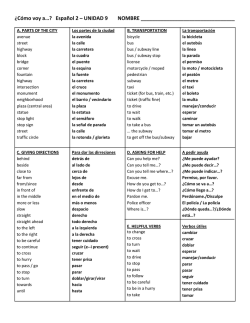

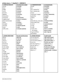
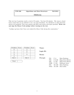

© Copyright 2026