
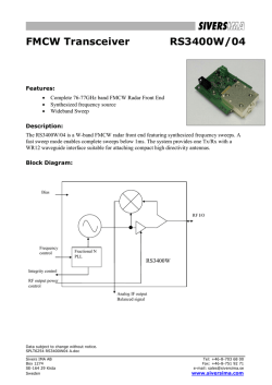
Quad 2-Input NAND Schmitt Trigger
MC74AC132, MC74ACT132
Quad 2-Input NAND Schmitt
Trigger
High−Performance Silicon−Gate CMOS
The MC74AC/74ACT132 contains four 2−input NAND gates
which are capable of transforming slowly changing input signals into
sharply defined, jitter−free output signals. In addition, they have
greater noise margin than conventional NAND gates.
Each circuit contains a 2−input Schmitt trigger. The Schmitt trigger
uses positive feedback to effectively speed−up slow input transitions,
and provide different input threshold voltages for positive and
negative-going transitions. This hysteresis between the positive−going
and negative−going input threshold is determined by resistor ratios
and is essentially insensitive to temperature and supply voltage
variations.
MARKING
DIAGRAM
14
14
SOIC−14
D SUFFIX
CASE 751A
Schmitt Trigger Inputs
Outputs Source/Sink 24 mA
′ACT132 Has TTL Compatible Inputs
These are Pb−Free Devices
xxx132G
AWLYWW
1
1
xxx
A
WL
Y
WW
G
Features
•
•
•
•
www.onsemi.com
= AC or ACT
= Assembly Location
= Wafer Lot
= Year
= Work Week
= Pb−Free Package
VCC
ORDERING INFORMATION
14
13
12
11
10
9
See detailed ordering and shipping information in the package
dimensions section on page 5 of this data sheet.
1
2
3
4
5
6
8
7
GND
Figure 1. Pinout; 14−Lead Packages Conductors
(Top View)
FUNCTION TABLE
Inputs
Output
A
B
Y
L
L
H
H
L
H
L
H
H
H
H
L
H = HIGH Voltage Level
L = LOW Voltage Level
© Semiconductor Components Industries, LLC, 2015
January, 2015 − Rev. 8
1
Publication Order Number:
MC74AC132/D
MC74AC132, MC74ACT132
MAXIMUM RATINGS
Symbol
Parameter
Value
Unit
*0.5 to )7.0
V
*0.5 v VI v VCC )0.5
V
*0.5 v VO v VCC )0.5
V
DC Input Diode Current
$20
mA
IOK
DC Output Diode Current
$50
mA
IO
DC Output Sink/Source Current
$50
mA
ICC
DC Supply Current per Output Pin
$50
mA
IGND
DC Ground Current per Output Pin
$50
mA
TSTG
Storage Temperature Range
*65 to )150
°C
TL
Lead temperature, 1 mm from Case for 10 Seconds
260
°C
TJ
Junction temperature under Bias
)150
°C
qJA
Thermal Resistance (Note 2)
125
°C/W
PD
Power Dissipation in Still Air at 85°C
125
mW
MSL
Moisture Sensitivity
FR
Flammability Rating
VESD
ESD Withstand Voltage
Human Body Model (Note 3)
Machine Model (Note 4)
Charged Device Model (Note 5)
> 2000
> 200
> 1000
V
ILatch−Up
Latch−Up Performance
Above VCC and Below GND at 85°C (Note 6)
$100
mA
VCC
DC Supply Voltage
VI
DC Input Voltage
VO
DC Output Voltage
IIK
(Note 1)
Level 1
Oxygen Index: 30% − 35%
UL 94 V−0 @ 0.125 in
Stresses exceeding those listed in the Maximum Ratings table may damage the device. If any of these limits are exceeded, device functionality
should not be assumed, damage may occur and reliability may be affected.
1. IO absolute maximum rating must be observed.
2. The package thermal impedance is calculated in accordance with JESD51−7.
3. Tested to EIA/JESD22−A114−A.
4. Tested to EIA/JESD22−A115−A.
5. Tested to JESD22−C101−A.
6. Tested to EIA/JESD78.
RECOMMENDED OPERATING CONDITIONS
Symbol
Parameter
VCC
Supply Voltage
Vin, Vout
DC Input Voltage, Output Voltage (Ref. to GND)
tr, tf
Input Rise and Fall Time (Note 1)
′AC Devices except Schmitt Inputs
Min
Typ
Max
Unit
′AC
2.0
5.0
6.0
′ACT
4.5
5.0
5.5
0
−
VCC
VCC @ 3.0 V
−
150
−
VCC @ 4.5 V
−
40
−
VCC @ 5.5 V
−
25
−
VCC @ 4.5 V
−
10
−
VCC @ 5.5 V
−
8.0
−
−
−
140
°C
−40
25
85
°C
V
V
ns/V
tr, tf
Input Rise and Fall Time (Note 2)
′ACT Devices except Schmitt Inputs
TJ
Junction Temperature (PDIP)
TA
Operating Ambient Temperature Range
IOH
Output Current − High
−
−
−24
mA
IOL
Output Current − Low
−
−
24
mA
ns/V
Functional operation above the stresses listed in the Recommended Operating Ranges is not implied. Extended exposure to stresses beyond
the Recommended Operating Ranges limits may affect device reliability.
1. Vin from 30% to 70% VCC; see individual Data Sheets for devices that differ from the typical input rise and fall times.
2. Vin from 0.8 V to 2.0 V; see individual Data Sheets for devices that differ from the typical input rise and fall times.
www.onsemi.com
2
MC74AC132, MC74ACT132
DC CHARACTERISTICS
Symbol
VOH
VOL
Parameter
Minimum High Level
Output Voltage
Maximum Low Level
Output Voltage
IIN
Maximum Input
Leakage Current
IOLD
†Minimum Dynamic
Output Current
IOHD
ICC
Maximum Quiescent
Supply Current
VCC
(V)
74AC
74AC
TA = +25°C
TA =
−40°C to
+85°C
Typ
Guaranteed Limits
3.0
4.5
5.5
2.99
4.49
5.49
2.9
4.4
5.4
2.9
4.4
5.4
3.0
4.5
5.5
−
−
−
2.56
3.86
4.86
2.46
3.76
4.76
3.0
4.5
5.5
0.002
0.001
0.001
0.1
0.1
0.1
0.1
0.1
0.1
3.0
4.5
5.5
−
−
−
0.36
0.36
0.36
0.44
0.44
0.44
5.5
−
±0.1
5.5
−
5.5
−
−
5.5
Unit
Conditions
IOUT = −50 mA
V
*VIN = VIL or VIH
−12 mA
IOH
−24 mA
−24 mA
V
IOUT = 50 mA
V
V
*VIN = VIL or VIH
12 mA
IOL
24 mA
24 mA
±1.0
mA
VI = VCC, GND
−
75
mA
VOLD = 1.65 V Max
−
−75
mA
VOHD = 3.85 V Min
4.0
40
mA
VIN = VCC or GND
Product parametric performance is indicated in the Electrical Characteristics for the listed test conditions, unless otherwise noted. Product
performance may not be indicated by the Electrical Characteristics if operated under different conditions.
*All outputs loaded; thresholds on input associated with output under test.
†Maximum test duration 2.0 ms, one output loaded at a time.
NOTE: IIN and ICC @ 3.0 V are guaranteed to be less than or equal to the respective limit @ 5.5 V VCC.
AC CHARACTERISTICS
Symbol
VCC*
(V)
Parameter
74AC
74AC
TA = +25°C
CL = 50 pF
TA = −40°C
to +85°C
CL = 50 pF
Min
Typ
Max
Min
Max
Unit
Fig.
No.
tPLH
Propagation Delay
3.3
5.0
2.0
2.0
−
−
13.0
9.0
1.5
1.5
14.0
10.0
ns
3−5
tPHL
Propagation Delay
3.3
5.0
2.0
2.0
−
−
13.5
9.0
1.5
1.5
15.0
10.0
ns
3−5
*Voltage Range 3.3 V is 3.3 V ±0.3 V.
Voltage Range 5.0 V is 5.0 V ±0.5 V.
www.onsemi.com
3
MC74AC132, MC74ACT132
DC CHARACTERISTICS
Symbol
VOH
VOL
Parameter
Minimum High Level
Output Voltage
Maximum Low Level
Output Voltage
VCC
(V)
74ACT
74ACT
TA = +25°C
TA =
−40°C to
+85°C
Unit
Conditions
Typ
Guaranteed Limits
4.5
5.5
4.49
5.49
4.4
5.4
4.4
5.4
4.5
5.5
−
−
3.86
4.86
3.76
4.76
4.5
5.5
0.001
0.001
0.1
0.1
0.1
0.1
4.5
5.5
−
−
0.36
0.36
0.44
0.44
V
*VIN = VIL or VIH
24 mA
IOL
24 mA
IOUT = −50 mA
V
*VIN = VIL or VIH
−24 mA
IOH
−24 mA
V
IOUT = 50 mA
V
IIN
Maximum Input
Leakage Current
5.5
−
±0.1
±1.0
mA
VI = VCC, GND
DICCT
Additional Max. ICC/Input
5.5
0.6
−
1.5
mA
VI = VCC − 2.1 V
IOLD
†Minimum Dynamic
Output Current
5.5
−
−
75
mA
VOLD = 1.65 V Max
5.5
−
−
−75
mA
VOHD = 3.85 V Min
5.5
−
4.0
40
mA
VIN = VCC or GND
IOHD
ICC
Maximum Quiescent
Supply Current
Product parametric performance is indicated in the Electrical Characteristics for the listed test conditions, unless otherwise noted. Product
performance may not be indicated by the Electrical Characteristics if operated under different conditions.
*All outputs loaded; thresholds on input associated with output under test.
†Maximum test duration 2.0 ms, one output loaded at a time.
AC CHARACTERISTICS
Symbol
VCC*
(V)
Parameter
74ACT
74ACT
TA = +25°C
CL = 50 pF
TA = −40°C
to +85°C
CL = 50 pF
Unit
Fig.
No.
Min
Typ
Max
Min
Max
tPLH
Propagation Delay
5.0
3.0
−
11.5
2.5
13.0
ns
3−6
tPHL
Propagation Delay
5.0
3.0
−
11.0
2.5
12.5
ns
3−5
*Voltage Range 5.0 V is 5.0 V ±0.5 V.
www.onsemi.com
4
MC74AC132, MC74ACT132
INPUT CHARACTERISTICS (unless otherwise specified)
Symbol
Parameter
VCC
(V)
74AC
74ACT
Unit
Test Conditions
Vt +
Maximum Positive
Threshold
3.0
4.5
5.5
2.2
3.2
3.9
2.0
V
TA = Worst Case
Vt −
Minimum Negative
Threshold
3.0
4.5
5.5
0.5
0.9
1.1
0.8
V
TA = Worst Case
Vh(max)
Maximum Hysteresis
3.0
4.5
5.5
1.2
1.4
1.6
1.2
V
TA = Worst Case
Vh(min)
Minimum Hysteresis
3.0
4.5
5.5
0.3
0.4
0.5
0.4
V
TA = Worst Case
CAPACITANCE
Symbol
Parameter
Value
Typ
Unit
Test Conditions
CIN
Input Capacitance
4.5
pF
VCC = 5.0 V
CPD
Power Dissipation Capacitance
30
pF
VCC = 5.0 V
ORDERING INFORMATION
Package
Shipping†
MC74AC132DG
SOIC−14
(Pb−Free)
55 Units/Rail
MC74AC132DR2G
SOIC−14
(Pb−Free)
2500/Tape & Reel
MC74ACT132DG
SOIC−14
(Pb−Free)
55 Units/Rail
MC74ACT132DR2G
SOIC−14
(Pb−Free)
2500/Tape & Reel
Device
†For information on tape and reel specifications, including part orientation and tape sizes, please refer to our Tape and Reel Packaging
Specifications Brochure, BRD8011/D.
www.onsemi.com
5
MC74AC132, MC74ACT132
PACKAGE DIMENSIONS
SOIC−14 NB
CASE 751A−03
ISSUE K
D
A
B
14
NOTES:
1. DIMENSIONING AND TOLERANCING PER
ASME Y14.5M, 1994.
2. CONTROLLING DIMENSION: MILLIMETERS.
3. DIMENSION b DOES NOT INCLUDE DAMBAR
PROTRUSION. ALLOWABLE PROTRUSION
SHALL BE 0.13 TOTAL IN EXCESS OF AT
MAXIMUM MATERIAL CONDITION.
4. DIMENSIONS D AND E DO NOT INCLUDE
MOLD PROTRUSIONS.
5. MAXIMUM MOLD PROTRUSION 0.15 PER
SIDE.
8
A3
E
H
L
1
0.25
M
DETAIL A
7
B
13X
M
b
0.25
M
C A
S
B
S
DETAIL A
h
A
X 45 _
M
A1
e
DIM
A
A1
A3
b
D
E
e
H
h
L
M
C
SEATING
PLANE
MILLIMETERS
MIN
MAX
1.35
1.75
0.10
0.25
0.19
0.25
0.35
0.49
8.55
8.75
3.80
4.00
1.27 BSC
5.80
6.20
0.25
0.50
0.40
1.25
0_
7_
INCHES
MIN
MAX
0.054 0.068
0.004 0.010
0.008 0.010
0.014 0.019
0.337 0.344
0.150 0.157
0.050 BSC
0.228 0.244
0.010 0.019
0.016 0.049
0_
7_
SOLDERING FOOTPRINT*
6.50
14X
1.18
1
1.27
PITCH
14X
0.58
DIMENSIONS: MILLIMETERS
*For additional information on our Pb−Free strategy and soldering
details, please download the ON Semiconductor Soldering and
Mounting Techniques Reference Manual, SOLDERRM/D.
ON Semiconductor and the
are registered trademarks of Semiconductor Components Industries, LLC (SCILLC) or its subsidiaries in the United States and/or other countries.
SCILLC owns the rights to a number of patents, trademarks, copyrights, trade secrets, and other intellectual property. A listing of SCILLC’s product/patent coverage may be accessed
at www.onsemi.com/site/pdf/Patent−Marking.pdf. SCILLC reserves the right to make changes without further notice to any products herein. SCILLC makes no warranty, representation
or guarantee regarding the suitability of its products for any particular purpose, nor does SCILLC assume any liability arising out of the application or use of any product or circuit, and
specifically disclaims any and all liability, including without limitation special, consequential or incidental damages. “Typical” parameters which may be provided in SCILLC data sheets
and/or specifications can and do vary in different applications and actual performance may vary over time. All operating parameters, including “Typicals” must be validated for each
customer application by customer’s technical experts. SCILLC does not convey any license under its patent rights nor the rights of others. SCILLC products are not designed, intended,
or authorized for use as components in systems intended for surgical implant into the body, or other applications intended to support or sustain life, or for any other application in which
the failure of the SCILLC product could create a situation where personal injury or death may occur. Should Buyer purchase or use SCILLC products for any such unintended or
unauthorized application, Buyer shall indemnify and hold SCILLC and its officers, employees, subsidiaries, affiliates, and distributors harmless against all claims, costs, damages, and
expenses, and reasonable attorney fees arising out of, directly or indirectly, any claim of personal injury or death associated with such unintended or unauthorized use, even if such claim
alleges that SCILLC was negligent regarding the design or manufacture of the part. SCILLC is an Equal Opportunity/Affirmative Action Employer. This literature is subject to all applicable
copyright laws and is not for resale in any manner.
PUBLICATION ORDERING INFORMATION
LITERATURE FULFILLMENT:
Literature Distribution Center for ON Semiconductor
P.O. Box 5163, Denver, Colorado 80217 USA
Phone: 303−675−2175 or 800−344−3860 Toll Free USA/Canada
Fax: 303−675−2176 or 800−344−3867 Toll Free USA/Canada
Email: [email protected]
N. American Technical Support: 800−282−9855 Toll Free
USA/Canada
Europe, Middle East and Africa Technical Support:
Phone: 421 33 790 2910
Japan Customer Focus Center
Phone: 81−3−5817−1050
www.onsemi.com
6
ON Semiconductor Website: www.onsemi.com
Order Literature: http://www.onsemi.com/orderlit
For additional information, please contact your local
Sales Representative
MC74AC132/D

© Copyright 2026