
Datasheet Template
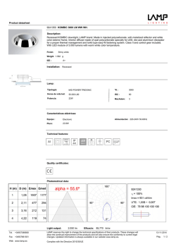
TGA2612 6-12 GHz GaN LNA Applications Commercial and Military Radar Communications Product Features Functional Block Diagram Frequency Range: 6–12GHz NF: < 1.8dB (1.5dB midband) P1dB: 20dBm OTOI: 29dBm Small Signal Gain: >22dB Return Loss: >7dB Bias: VD = 10V, IDQ = 100mA, VG = -2.3V Typical Chip Dimensions: 2.1 x 1.5 x 0.10mm 2 J1 RF In 1 3 J2 RF Out 4 Performance features are typical across frequency, under recommended bias and at 25°C carrier backside. General Description Pad Configuration TriQuint’s TGA2612 is a broadband Low Noise Amplifier fabricated on TriQuint’s production 0.25um GaN on SiC process (TQGaN25). Covering 6–12GHz, the TGA2612 typically provides P1dB of 20dBm, greater than 22dB of small signal gain, 1.5dB noise figure (mid-band) and 29dBm OTOI. In addition to the high electrical performance, this GaN amplifier also provides a high level of input power robustness. Able to survive up to 2W of input power without performance degradation, TriQuint’s TGA2612 provides flexibility regarding receive chain protection resulting in lower costs and reduced board space. Fully matched to 50 ohms with integrated DC blocking caps on both I/O ports, the TGA2612 is ideally suited for both military and commercial radar and communications applications. Lead-free and RoHS compliant Evaluation Boards are available upon request. Preliminary Datasheet: Rev - 01-21-14 © 2014 TriQuint Pad No. Symbol 1 2 3 4 RF In VD RF Out VG Ordering Information Part TGA2612 - 1 of 12 - ECCN EAR99 Description 6 – 12 GHz GaN LNA Disclaimer: Subject to change without notice www.triquint.com TGA2612 6-12 GHz GaN LNA Absolute Maximum Ratings Parameter Value Drain Voltage (VD) Gate Voltage Range (VG) Drain Current (ID) Gate Current (IG) Power Dissipation, 85 °C (PDISS) Input Power, CW, 50 Ω, (PIN) Channel temperature (TCH) 40V -5 to 0V 250mA -1 to 7mA 6W 34dBm 275°C Mounting Temperature (30 Seconds) Storage Temperature Recommended Operating Conditions Parameter Value Drain Voltage (VD) Drain Current (IDQ) Gate Voltage (VG) 10V 100mA -2.3V Typical Electrical specifications are measured at specified test conditions. Specifications are not guaranteed overall operating conditions. 320°C -55 to 150°C Operation of this device outside the parameter ranges given above may cause permanent damage. These are stress ratings only, and functional operation of the device at these conditions is not implied. Electrical Specifications 0 Test conditions unless otherwise noted: 25 C, VD = 10V, IDQ = 100mA, VG = -2.3V Typical Parameter Operation Frequency Range Small Signal Gain Input Return Loss Output Return Loss Noise Figure Output Power at 1 dB Gain Compression Output TOI Gain Temperature Coefficient Noise Figure Temperature Coefficient Preliminary Datasheet: Rev - 01-21-14 © 2014 TriQuint Min Typical 6.0 >22 >7 >10 <1.8 20 29 -0.044 -0.009 - 2 of 12 - Max Units 12.0 GHz dB dB dB dB dBm dBm dB/°C dB/°C Disclaimer: Subject to change without notice www.triquint.com TGA2612 6-12 GHz GaN LNA Thermal and Reliability Information Parameter Test Conditions (1) Thermal Resistance (θJC) Channel Temperature, TCH (Without RF) Median Lifetime (TM) Value 16 Tbaseplate = 85°C, VD = 10V, IDQ = 100mA, 101 PDISS =1W 7.9 x 10^11 (1) Thermal Resistance (θJC) Channel Temperature, TCH (Under RF) Median Lifetime (TM) Tbaseplate = 85°C, VD = 10V, ID_Drive = 208mA, POUT = 26.6dBm, PDISS = 1.6W 16 111 2 x 10^11 Units ºC/W °C Hrs ºC/W °C Hrs Notes: 1. Thermal resistance measured to back of carrier plate. MMIC mounted on 40 mils CuMo carrier using 1.5 mil 80/20 AuSn. Median Lifetime Test Conditions: VD = 40V; Failure Criteria is 10% reduction in ID_MAX Preliminary Datasheet: Rev - 01-21-14 © 2014 TriQuint - 3 of 12 - Disclaimer: Subject to change without notice www.triquint.com TGA2612 6-12 GHz GaN LNA Typical Performance Conditions unless otherwise specified: VD = 10V, IDQ = 100mA, VG = -2.3V Typical Gain vs. Frequency vs. Temperature 34.0 Input Return Loss vs. Freq. vs. Temp. 0 - 40 °C 30.0 -5 26.0 -10 +25 °C S11 (dB) S21 (dB) +85 °C 22.0 18.0 -15 -20 - 40 °C 14.0 -25 +25 °C +85 °C 10.0 -30 5.0 6.0 7.0 8.0 9.0 10.0 11.0 12.0 13.0 5.0 6.0 7.0 8.0 Frequency (GHz) Output Return Loss vs. Freq. vs. Temp. 0 9.0 10.0 11.0 -5 30.0 -10 26.0 S21 (dB) S22 (dB) 13.0 Gain vs. Frequency vs. VD 34.0 IDQ = 100mA Temp. = 25 C -15 22.0 20V 18V 16V 14V 12V 10V 18.0 -20 - 40 °C +25 °C -25 14.0 +85 °C 10.0 -30 5.0 6.0 7.0 8.0 9.0 10.0 11.0 12.0 5.0 13.0 6.0 7.0 Frequency (GHz) 8.0 9.0 12.0 13.0 -40 C 30.0 Noise Figure (dB) 3 26.0 22.0 140mA 120mA 100mA 80mA 60mA 14.0 11.0 Noise Figure vs. Freq. vs. Temperature 3.5 VD = 10V Temp. = 25 C 18.0 10.0 Frequency (GHz) Gain vs. Frequency vs. IDQ 34.0 S21 (dB) 12.0 Frequency (GHz) +25 °C +85 °C 2.5 2 1.5 1 VD = 10 V, IDQ = 100mA 10.0 0.5 5.0 6.0 7.0 8.0 9.0 10.0 11.0 12.0 13.0 5.0 Preliminary Datasheet: Rev - 01-21-14 © 2014 TriQuint 6.0 7.0 8.0 9.0 10.0 11.0 12.0 13.0 Frequency (GHz) Frequency (GHz) - 4 of 12 - Disclaimer: Subject to change without notice www.triquint.com TGA2612 6-12 GHz GaN LNA Typical Performance Conditions Conditionsunless unlessotherwise otherwisespecified: specified:VVDD==10 10V, V, IIDQ DQ = = 125 100mA, mA, V VGG == -2.3V -2.3 VTypical Typical Noise Figure vs. Frequency. vs. VD 3 Temp. = +25 °C 2.8 Temp. = +25 °C VD = 10 V 2.8 2.6 Noise Figure (dB) 2.6 Noise Figure (dB) Noise Figure vs. Frequency vs. IDQ 3 IDQ = 100mA 2.4 2.2 2 1.8 1.6 1.4 2.4 2.2 2 1.8 1.6 1.4 6V 1.2 10V 12V 14V 16V 18V 20V 1.2 1 IDQ=60mA IDQ=80mA IDQ=100mA IDQ=120mA IDQ=140mA 1 5.0 6.0 7.0 8.0 9.0 10.0 11.0 12.0 13.0 5.0 6.0 7.0 Frequency (GHz) PSAT vs. Frequency vs. Temperature 9.0 10.0 11.0 13.0 PSAT vs. Frequency. vs. VD 32 30 29 28 26 26 24 23 6V 8V 10V 12V 14V 16V 18V 20V 20 - 40 °C +25 °C 22 17 +85 °C PIN = 12dBm Temp. = +25 °C IDQ = 100 mA, PIN = 12dBm 14 20 5.0 6.0 7.0 8.0 9.0 10.0 11.0 12.0 5.0 13.0 6.0 7.0 P1dB vs. Frequency vs. Temperature 25 8.0 9.0 10.0 11.0 13.0 P1dB vs. Frequency. vs. VD 25 Temp. = +25 °C VD = 10 V, IDQ = 100 mA 22 21 19 P1dB (dBm) 23 19 17 16 6V 8V 10V 12V 14V 16V 18V 20V 13 - 40 °C +25 °C 15 12.0 Frequency (GHz) Frequency (GHz) P1dB (dBm) 12.0 VD = 10 V, IDQ = 100 mA PSAT (dBm) PSAT (dBm) 32 8.0 Frequency (GHz) 10 +85 °C IDQ = 100 mA 13 7 5.0 6.0 7.0 8.0 9.0 10.0 11.0 12.0 13.0 5.0 Frequency (GHz) Preliminary Datasheet: Rev - 01-21-14 © 2014 TriQuint 6.0 7.0 8.0 9.0 10.0 11.0 12.0 13.0 Frequency (GHz) - 5 of 12 - Disclaimer: Subject to change without notice www.triquint.com TGA2612 6-12 GHz GaN LNA Typical Performance Conditions unless otherwise specified: VD = 10V, IDQ = 100mA, VG = -2.3V Typical Gain vs. Input Power vs. Frequency 30 Temp. = +25 °C Temp. = +25 °C 27 VD = 10 V, IDQ = 100 mA 230 Drain Current (mA) Gain (dB) ID vs. Input Power vs. Frequency 260 VD = 10 V, IDQ = 100 mA 24 21 18 6.0 GHz 8.0 GHz 15 200 6.0 GHz 170 10.0 GHz 12.0 GHz 8.0 GHz 140 110 10.0 GHz 12.0 GHz 12 80 -15 -12 -9 -6 -3 0 3 6 9 12 -15 -12 -9 Input Power (dBm) -6 -3 0 3 6 9 12 Input Power (dBm) Output Power vs. Input Power vs. VD. 32 IDQ = 100mA Temp. = +25 °C Output Power (dBm) 28 24 20 6V 8V 10V 12V 14V 16V 18V 20V 16 12 Frequency = 9 GHz 8 -15 -12 -9 -6 -3 0 3 6 9 12 Input Power (dBm) OTOI vs. Frequency vs. Temperature 35 33 29 31 OTOI (dBm) OTOI (dBm) PIN =-20 dBm, 10 MHz Tone Spacing Temp. = +25 °C 32 26 23 OTOI vs. Frequency vs. VD 35 PIN =-20 dBm, 10 MHz Tone Spacing - 40 °C 29 6V 8V 10V 12V 14V 27 +25 °C 20 25 +85 °C VD = 10V, IDQ = 100mA IDQ = 100mA 17 23 6.0 7.0 8.0 9.0 10.0 11.0 12.0 6.0 Frequency (GHz) Preliminary Datasheet: Rev - 01-21-14 © 2014 TriQuint 7.0 8.0 9.0 10.0 11.0 12.0 Frequency (GHz) - 6 of 12 - Disclaimer: Subject to change without notice www.triquint.com TGA2612 6-12 GHz GaN LNA Typical Performance Conditions unless otherwise specified: VD = 10V, IDQ = 100mA, VG = -2.3V Typical OTOI vs. Frequency vs. ID 38 PIN = -20 dBm, 10 MHz Tone Spacing 35 -40 32 -50 29 IDQ=60mA 26 IDQ=100mA IDQ=120mA IDQ=140mA 23 20 7.0 8.0 9.0 10.0 11.0 -60 -70 IDQ=80mA 6.0 IM3 vs. Frequency vs. Temperature -30 VD = 10V, PIN =-20 dBm, 10 MHz Tone Spacing IM3 (dBc) OTOI (dBm) Temp. = +25 °C - 40 °C +25 °C -80 +85 °C VD = 10V, IDQ = 100mA -90 12.0 6.0 7.0 8.0 Frequency (GHz) IM3 vs. Output Power vs. Frequency 0 Temp. = +25 °C 12.0 VD = 10 V, IDQ = 100 mA, 10 MHz Tone Spacing -10 6 GHz 8 GHz -20 11.0 -20 10 GHz IM3 (dBc) IM3 (dBc) -10 10.0 IM3 vs. Input Power vs. Frequency 0 VD = 10 V, IDQ = 100 mA, 10 MHz Tone Spacing Temp. = +25 °C 9.0 Frequency (GHz) 12 GHz -30 -30 -40 -40 -50 -50 6 GHz 8 GHz 10 GHz 12 GHz -60 -60 2 4 6 8 10 12 14 16 18 20 22 -20 Output Power per Tone (dBm) Preliminary Datasheet: Rev - 01-21-14 © 2014 TriQuint -16 -12 -8 -4 0 4 8 12 Input Power per Tone (dBm) - 7 of 12 - Disclaimer: Subject to change without notice www.triquint.com TGA2612 6-12 GHz GaN LNA Application Circuit C10 0.01 uF 2 VD = 10 V, IDQ = 100 mA 1 J1 RF In 3 J2 RF Out 4 VG = -2.3 V Typical R8 4 Ohm C8 1 uF C12 0.01 uF Bias-up Procedure Bias-down Procedure 1. Set ID limit to 230mA, IG limit to 1mA 2. Apply -5V to VG for pinch off 3. Apply +10V to VD 1. Turn off RF signal 2. Reduce VG to -5V. Ensure IDQ ~ 0mA 3. Set VD to 0V 4. Adjust VG more positive until IDQ = 100mA (VG ~ -2.3 V Typical) 4. Turn off VD supply 5. Apply RF signal 5. Turn off VG supply Preliminary Datasheet: Rev - 01-21-14 © 2014 TriQuint - 8 of 12 - Disclaimer: Subject to change without notice www.triquint.com TGA2612 6-12 GHz GaN LNA Assembly Drawing VD = 10 V, IDQ = 100 mA C10 0.01 uF RF In 2 RF Out 3 1 4 VG = -2.3 V Typical R8 4 Ohm C8 1 uF Preliminary Datasheet: Rev - 01-21-14 © 2014 TriQuint C12 0.01 uF - 9 of 12 - Disclaimer: Subject to change without notice www.triquint.com TGA2612 6-12 GHz GaN LNA Mechanical Drawing & Bond Pad Description 2 3 1 4 Unit: millimeters Thickness: 0.10 Die x, y size tolerance: +/- 0.050 Chip edge to bond pad dimensions are shown to center of pad Ground is backside of die Bond Pad Symbol 1 RF In 0.098 x 0.198 2 VD 0.098 x 0.098 Input; matched to 50 ohms Drain voltage, VD. Bias network is required; see Application Circuit on page 8 as an example. 3 RF Out 0.098 x 0.198 Output; matched to 50 ohms 4 VG 0.098 x 0.098 Gate voltage, VG. Bias network is required; see Application Circuit on page 8 as an example. Preliminary Datasheet: Rev - 01-21-14 © 2014 TriQuint Pad Size Description - 10 of 12 - Disclaimer: Subject to change without notice www.triquint.com TGA2612 6-12 GHz GaN LNA Assembly Notes Component placement and adhesive attachment assembly notes: • Vacuum pencils and/or vacuum collets are the preferred method of pick up. • Air bridges must be avoided during placement. • The force impact is critical during auto placement. • Organic attachment (i.e. epoxy) can be used in low-power applications. • Curing should be done in a convection oven; proper exhaust is a safety concern. Reflow process assembly notes: • Use AuSn (80/20) solder and limit exposure to temperatures above 300C to 3-4 minutes, maximum. • An alloy station or conveyor furnace with reducing atmosphere should be used. • Do not use any kind of flux. • Coefficient of thermal expansion matching is critical for long-term reliability. • Devices must be stored in a dry nitrogen atmosphere. Interconnect process assembly notes: • Thermosonic ball bonding is the preferred interconnect technique. • Force, time, and ultrasonic are critical parameters. • Aluminum wire should not be used. • Devices with small pad sizes should be bonded with 0.0007-inch wire. Preliminary Datasheet: Rev - 01-21-14 © 2014 TriQuint - 11 of 12 - Disclaimer: Subject to change without notice www.triquint.com TGA2612 6-12 GHz GaN LNA Product Compliance Information ESD Sensitivity Ratings Solderability Caution! ESD-Sensitive Device This part is compliant with EU 2002/95/EC RoHS directive (Restrictions on the Use of Certain Hazardous Substances in Electrical and Electronic Equipment). This product also has the following attributes: Lead Free Halogen Free (Chlorine, Bromine) Antimony Free TBBP-A (C15H12Br402) Free PFOS Free SVHC Free ESD Rating: TBD Value: TBD Test: Human Body Model (HBM) Standard: JEDEC Standard JESD22-A114 ECCN US Department of Commerce: EAR99 Contact Information For the latest specifications, additional product information, worldwide sales and distribution locations, and information about TriQuint: Web: www.triquint.com Email: [email protected] Tel: Fax: For technical questions and application information: +1.972.994.8465 +1.972.994.8504 Email: [email protected] Important Notice The information contained herein is believed to be reliable. TriQuint makes no warranties regarding the information contained herein. TriQuint assumes no responsibility or liability whatsoever for any of the information contained herein. TriQuint assumes no responsibility or liability whatsoever for the use of the information contained herein. The information contained herein is provided "AS IS, WHERE IS" and with all faults, and the entire risk associated with such information is entirely with the user. All information contained herein is subject to change without notice. Customers should obtain and verify the latest relevant information before placing orders for TriQuint products. The information contained herein or any use of such information does not grant, explicitly or implicitly, to any party any patent rights, licenses, or any other intellectual property rights, whether with regard to such information itself or anything described by such information. TriQuint products are not warranted or authorized for use as critical components in medical, life-saving, or lifesustaining applications, or other applications where a failure would reasonably be expected to cause severe personal injury or death. Preliminary Datasheet: Rev - 01-21-14 © 2014 TriQuint - 12 of 12 - Disclaimer: Subject to change without notice www.triquint.com

© Copyright 2026