
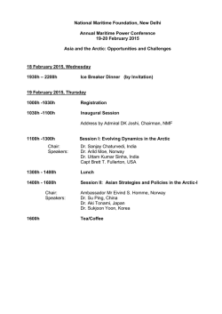
SCIENTIFIC PROGRAM (Click to download)
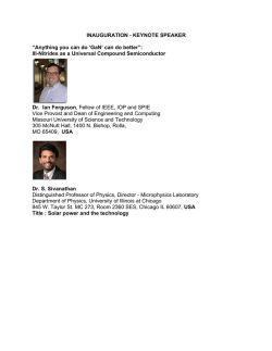
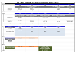
02 February 2015 (Monday)
Inauguration ( 09300 to 10.30 )
High Tea ( 10.30 to 11.00 )
KEYNOTE SPEAKERS
Session Chair : Dr Vikram Kumar
Dr. I. Ferguson
“Anything you can do ‘GaN’ can do
Missouri University of Science
better”: III-Nitrides as a Universal
and Technology Rolla
Compound Semiconductor
USA.
Dr. S. Sivanathan
Solar Power and the Technology
University of Illinois, Chicago
USA.
Dr. Ramgopal Rao
Bottom-up meets Top-down: An Integrated
IIT Bombay, Mumbai
Approach for Future Nanoscale Devices
India
13.15-14.00 (Lunch)
Dr. T. Kuech
University of Wisconsin
Madison,USA
Dr. M. Kuball
University of Bristol
United Kingdom
11.00-11.45
11.45-12.30
12.30-13.15
Session Chair : Dr. J. Kumar
Vapor Phase Growth of Complex and
Metastable Semiconductor Alloys
14.00-14.30
Challenges for GaN Electronics - Of
Dragons and Knights
14.30-15.00
15.00-15.15 (Tea)
Session Chair : Dr. R. Dhanasekaran
Dr. Ng Geok Ing
Towards Cost-Effective HEMTs: Are We
Silicon Technologies Centre of
There Yet?
Excellence Nanyang
Technological University,
Singapore
Dr. Arnab Bhattacharya
Tata Institute of Fundamental
MOVPE growth of III-nitrides on 2D
Research, Mumbai
layered materials
India
Poster Session (Please see your poster presentation schedule on
www.issmd.org website)
15.15-16.00
16.00 - 16.30
16.30-18.00
03 February 2015 (Tuesday)
Dr. M. Pons
Institut Polytechnique de
Grenoble
France
Session Chair : Dr. K. Baskar
Functional properties and microstructure of
AlN thin films and coatings grown by CVD
Dr.Gen Sazaki
Hokkaido University,
Japan
Direct visualization of surface melting
processes: an example found on ice crystal
surfaces
Dr. J. V. Kennedy
National Isotope Centre
New Zealand
Electronic, magneto transport and magnetic
properties of Gadolinium doped zinc oxide
09.00 – 09.45
09.45-10.30
10.30 - 11.00
11.00-11.15 (Tea)
Dr. A. A. Crisci
Institut Polytechnique de
Grenoble
France
Dr. T. W. Kang
Dongguk University
Korea
Dr. S. Raghavan
Indian Institute of Science,
Bangalore, India
Dr. H. Tan
Australian National University
Canberra
Australia
Dr. V. Gupta
University of Delhi
New Delhi, India
Dr. Rajendra Singh
IIT Delhi
India
Dr. A. Bhattacharya
Calcutta University
India
Session Chair :Dr. M. Pons
Contribution of Electron Probe Microanalysis
(EPMA) to the characterisation scheme of
thin layers
Study on Properties and Applications of II-VI
Nanostructures
Controlling Growth of Graphene and MoS2
12.45-14.00 (Lunch)
Session Chair : Dr. A.A. Crisci
Semiconductor nanowires for optoelectronic
device applications
Development of multifunctional materials for
electronic devices
15.00-15.15 (Tea)
Session Chair : Dr. S. MoorthyBabu
Fabrication and Characterization of GaN
nanopillars for Applications in Nanoscale
Devices
AlGaN alloys and their applications in
Ultraviolet Detectors
Dr. S. Mahapatra
Macroscopic and Stochastic Aspects of
IIT Bombay
Negative Bias Temperature Instability in
India
CMOS Devices and Circuits
Poster ( Please see your poster presentation schedule on www.issmd.org
website )
11.15-11.45
11.45-12.15
12.15 – 12.45
14.00 - 14.30
14.30 - 15.00
15.15 - 15.45
15.45 - 16.15
16515 - 16.45
16.45 - 18.00
04 February 2014 (Wednesday)
Dr. H. K. Lipsanen
Aalto University
Finland
Dr. L. Lazzarini
IMEM – Pharma
Italy
Dr. Eric Faulques
Université de Nantes
France
Dr. Shin Yokoyama
Hiroshima University,
Japan
Dr. J. Kumar
Anna University
India
Dr. Nandita Dasgupta
IIT Madras
India
Session Chair : Dr. Sazaki
III-V
semiconductor
nanowires
nanotechnology applications
for
Crystal
structure
assessment
of
nanostructured
GeSbTe-based
Phase
Change
Materials
by
Advanced
Transmission
Electron
Microscopy
techniques
10.15-10.30 (Tea)
Session Chair : Dr. Lipsanen
Studies of crystalline nanowires grown
inside carbon nanotubes
Si Ring Resonator and Photonic Crystal
Resonator Biosensors
On Dilute Magnetic Semiconductor related
issues in GaN
III Nitride MIS-HEMTs - Two approaches
to reduce leakage
09.00 - 09.45
09.45-10.15
10.30 - 11.15
11.15 - 12.00
12.00 - 12.30
12.30 - 13.00
13.00-14.00 (Lunch)
Dr. R. Jeyavel
Anna University, Chennai
India
Dr. R. Jeyakumar
National Physical Laboratory
New Delhi, India
Session Chair : Dr. Yokoyama
Development of nanohybrid structures for
dye sensitised and quantum dot sensitised
solar cell applications
Fabrication of c-Si solar cells using spin-on
dopants
14.00 – 14.30
14.30 - 15.00
15.00-15.15 (Tea)
Session Chair : Dr. L. Lazzarini
Dr. A. P. Pathak
Ion Beam Studies of Semiconductor
University of Hyderabad
Nanostructures
Hyderabad, India
Dr S K Srivastava
Silicon Nanowires: A potential approach
National Physical Laboratory
for efficient solar cells
New Delhi, India
Poster (Please see your poster presentation schedule on www.issmd.org
website)
15.15 - 15.45
15.45 - 16.15
16.15 - 18.00
05 February 2014 (Thrusday)
Dr. M. Henini
University of Nottingham
United Kingdom
Dr. Govind Gupta
National Physical Laboratory
New Delhi, India
Dr. K Jeganathan
Bharadhidasan University,
Trichy, India
Session Chair : Dr. H. Tan
Development of Advanced Semiconductor
Materials and Devices For Next Generation
Photovoltaics:
Opportunities
And
Challenges
High quality GaN films grown on different
substrates by molecular beam epiatxy
09.30 – 10.00
Lattice matched and strained growth of
InAlN/GaNheterostructure
10.00 – 10.30
09.00 - 09.45
10.30-10.45 (Tea)
Dr. Jesbains Kaur
University of Technology
Malaysia
Dr. K. Baskar
Anna University, Chennai
India
Dr. S. Suresh
CNRS, Metz, France
Dr. Ramachandra Rao
IIT, Chennai
India
Session Chair : Dr. S. N. Kalkura
Dependence of microstructures in MOVPEAlN on annealing temperature of sapphire
substrate
AlInGaN/AlN/GaN heterostructures grown
by MOCVD
Nano selective area growth of III-nitrides
for next generation devices
Electrical transport and optical properties
of metal-oxide thin films, heterostructures
and nanostructures
12.45-14.00 (Lunch)
Concluding Session – Valedictory
10.45 – 11.15
11.15 – 11.45
1!.45 – 12.15
12.15 – 12.45
14.00 – 15.00


© Copyright 2026