
Exploiting PV Inverters to Support Local Voltage—A Small
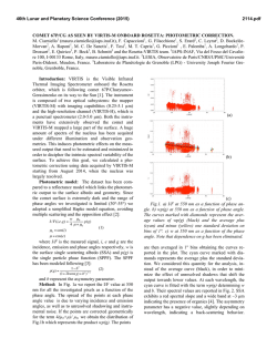
This article has been accepted for inclusion in a future issue of this journal. Content is final as presented, with the exception of pagination.
IEEE TRANSACTIONS ON ENERGY CONVERSION
1
Exploiting PV Inverters to Support Local Voltage—A
Small-Signal Model
Meghdad Fazeli, Member, IEEE, Janaka B. Ekanayake, Senior Member, IEEE, Paul M. Holland, Member, IEEE,
and Petar Igic, Member, IEEE
Abstract—As penetration of distributed generation increases,
the electrical distribution networks may encounter several challenges mainly related to voltage control. The situation may deteriorate in case of a weak grid connected to an intermittent source such
as photovoltaic (PV) generation. Fast varying solar irradiance can
cause unacceptable voltage variations that may not be easily compensated by slow-responding utility equipment. The PV inverter
can be used to control the grid voltage by injecting/absorbing reactive power. A small-signal model is derived in order to study
the stability of a PV inverter exchanging reactive power with the
grid. This paper also proposes a method that utilizes the available
capacity of the PV inverter to support the grid voltage without violating the rating of the inverter and the maximum voltage that the
inverter’s switching device can withstand. The method proposed
in this paper is validated using PSCAD/EMTDC simulations.
Index Terms—Distributed generation (DG), photovoltaic (PV)
system, voltage control.
I. INTRODUCTION
ISTRIBUTED generation (DG) benefits the electric utility by reducing congestion on the grid, decreasing the
need for new generation and transmission capacity and (potentially) can offer services such as local frequency and voltage
support/control [1]–[5]. However, as penetration of renewablebased DG increases, the intermittent nature of the source can
cause challenges such as voltage variations which in turn can
lead to system instability [6]. Yan and Saha [7] investigate the
IEEE 13 nodes test system with different level of photovoltaic
(PV) penetrations and show for a penetration more than 40%; the
voltage fluctuations introduced by passing clouds may make the
system unstable. In such situations, the slow-responding equipment (e.g., tap changers or switchable capacitors) may not be
effective in controlling the voltage within its limits [6], [8]. For
instance, it takes 5–10 s for the tap changer to move from one position to the next [7]. Relying on the tap changer in a fast varying
irradiance condition, (assuming is practically possible) will also
D
Manuscript received July 5, 2013; revised November 18, 2013; accepted
December 16, 2013. This work was sponsored by European Regional Development Fund through Welsh European Funding Office, Welsh Government. Paper
no. TEC-00380-2013.
M. Fazeli, P. M. Holland, and P. Igic are with the Electronic Design Center,
College of Engineering, Swansea University, Swansea SA2 9HD, U.K.
(e-mail: [email protected]; [email protected]; p.igic@
swansea.ac.uk).
J. B. Ekanayake is with the School of Engineering, Cardiff University, Cardiff
CF24 3AA, U.K. (e-mail: [email protected]).
Color versions of one or more of the figures in this paper are available online
at http://ieeexplore.ieee.org.
Digital Object Identifier 10.1109/TEC.2014.2300012
significantly reduce the interval between maintenance and increases the cost [9]. In addition to the slow response and the fact
that capacitor banks can generate high frequency harmonics,
switching the capacitor banks on/off produces a strong transient voltage variation that can damage other equipment (e.g.,
PV inverters) [6]. On the other hand, installing fast-responding
FACTS devices (e.g., STATCOM, SVC, etc.) will increase the
cost of already expensive PV systems [6]. Alternatively, it is
possible to utilize the PV inverter in order to control the voltage
within its limits through absorbing/injecting reactive power.
“Although it is not permitted by current interconnection standard [8], changes to these standards to allow for injecting or
consuming reactive power appear eminent” [6].
The allowed penetration level of (PV) DG is a controversial
issue among scientists [10] and varies from 5% [11], [12] to
33% [13] in the literature. Quezada et al. [12] suggest that the
loss in a distribution system is minimized at 5% penetration
of DG. However, the findings of [12] can be doubted if the
reactive power capacity of the PV inverter is exploited. For
instance, Turitsyn et al. [14] show that a localized approach
to supply reactive power (e.g., using PV inverters) can reduce
losses by up to 80% when compared to a centralized approach.
Thomson and Infield [13] study the voltage rise issue versus
the penetration level of PV generation into a UK distribution
network and conclude that for a PV generation up to 33%,
the voltage rise is within acceptable limits. However, Thomson
and Infield [13] also show that even at 50% penetration of PV
generation, the voltage rise above the allowed limit is small and
hence the 33% is rather arbitrary. From the findings of [13], it
can be suggested that by exploiting the PV inverters to support
the local voltage, it is possible to increase the penetration of
PV generation by more than 33%. It is noted that Thomson and
Infield [13] study the voltage rise issue due to a high penetration
of PV generation and it states that the voltage dips caused by
passing clouds can be significant. The current paper studies
a distribution system with 50% penetration of PV generation
(since it seems the maximum level suggested by the literature
[13]).
Turitsyn et al. [6] propose a voltage-reactive power droop
that utilizes the PV inverter to support voltage. The main drawback of the proposed method in [6] is that the reactive power
exchanged by the inverter never becomes zero even when the
voltage is within an acceptable boundary (which may introduce unnecessary losses). A similar method is proposed in [7]
with zero reactive power boundary; however, the mathematical
model of the system has not been investigated. Moreover, these
methods do not take into account the voltage rise issue due to
0885-8969 © 2014 IEEE. Personal use is permitted, but republication/redistribution requires IEEE permission.
See http://www.ieee.org/publications standards/publications/rights/index.html for more information.
This article has been accepted for inclusion in a future issue of this journal. Content is final as presented, with the exception of pagination.
2
Fig. 1.
IEEE TRANSACTIONS ON ENERGY CONVERSION
Configuration of the system under study.
the reverse active and reactive power flow. Beside the possibility
of exceeding the voltage limits, the voltage rise introduced by
PV inverters may cause “overmodulation” [15] (i.e., modulation index > 1), and even may harm the switching device (for a
constant dc-link voltage).
The papers in this area, such as [6], [7], [16], [17], do not study
the small-signal stability of a PV inverter exchanging reactive
power with the grid; which will be considered in this paper.
The paper also proposes a method that utilizes the available
capacity of the PV inverter(s) to support the grid voltage without
violating the rating of the inverter and the maximum voltage that
the inverter’s switching device can withstand.
The method will be developed for one PV inverter and
will be demonstrated for multiple PV inverters as well, using
PSCAD/EMTDC simulations.
II. SYSTEM UNDER STUDY
Fig. 1 shows the configuration of the system under study. It
illustrates that the PV array can supply maximum 50% of the full
load (at solar irradiation G = 1 kW/m2 ). The PV system utilizes
a single stage conversion using a three-phase dc/ac converter.
The converter is controlled using a dq rotating frame with the
d axes orientated along the filter voltage V2 . The d-component
current controls the dc-link voltage VDC in order to track the
maximum solar power (using the method explained in [18])
and the q-component controls the reactive power to/from the
converter. Park transformation is used to transfer variables from
abc to dq frame [19]. lC is the length of the cable connecting
the PV system to the grid and L1 , L2 , and C represent the filter
and Lg is the grid inductance.
A. Problem Definition
It can be shown that without any voltage support, the voltage
of point of common coupling VL < 0.94 pu for short-circuit
ratio (SCR) < 15 and in fact it drops to 0.87 pu for SCR = 5.
On the other hand, keeping VL at 1 pu using the PV inverter will
cause the inverter ac terminal voltage V1 to increase even more
than 1.2 pu. Therefore, a variable approach to control VL , as
illustrated in Fig. 1, seems to be more appropriate. The proposed
method exploits the available capacity of the PV inverter to
support the local voltage without violating either the rating of
the inverter or its voltage limitations. As QPV varies, both V1 and
Fig. 2.
Proposed Q–V droop characteristic.
the load voltage VL will be affected. Therefore, it is important
to choose a proper reactive power reference Q∗PV . In order to
choose a proper Q∗PV , the following constraints are considered.
1) Voltage of 11 kV busbar VL should be within ±6% (i.e.,
0.94 pu ≤ VL ≤ 1.06 pu) [20].
2) The maximum voltage that the switching device can withstand is 10% of its rated value (i.e., V1 ≤ 1.1 pu).
3) Rating of the inverter Snom should not be violated. Here
Snom = 1.2 pupv (pupv denotes pu based on the rating
of the associated PV array in systems with multiple PV
arrays).
B. Control Paradigm
Fig. 1 illustrates the proposed method to set Q∗PV in order
to support VL (if required) without violating Snom and V1 . The
method consists of three parts.
1) A PI controller which controls QPV through regulating the
q-component of converter current I1q , and is explained in
Section VI.
2) A variable hard limit which limits Q∗PV to makes sure
Snom is not exceeded.
3) Since the PV power PPV is intermittent, the maximum
reactive power that can be exchanged by the inverter is
2 , hence a variable
2
Snom
− PPV
varying as: Qm ax =
hard limit is required. Using the variable hard limit also
makes sure that the voltage support does not interfere with
the maximum power tracking.
Two reactive power-voltage droop characteristics for VL and
V1 as shown in Fig. 1 and illustrated in Fig. 2. These droops
provide the opportunity to keep QPV = 0 when the voltage is
within an acceptable boundary.
Fig. 2 illustrates the droop characteristics used for both VL
and V1 ; however, Vm in and Vm ax are different for each voltage.
This article has been accepted for inclusion in a future issue of this journal. Content is final as presented, with the exception of pagination.
FAZELI et al.: EXPLOITING PV INVERTERS TO SUPPORT LOCAL VOLTAGE—A SMALL-SIGNAL MODEL
Vm ax for V1 and VL is 1.1 and 1.06 pu, respectively. Vm in for
VPV and VL is 0.9 and 0.94 pu, respectively. As ΔV reduces,
the droop’s gain increases (for a given Snom ) which requires
a QPV control loop with higher bandwidth (which can cause
large voltage transient). On the other hand, the smaller ΔV , the
larger the boundary with zero reactive power (which reduces the
losses). So the choice of ΔV is a tradeoff between less loss and
less transient. Here, ΔV is chosen as 0.02 pu for both droops;
however, it can be different for V1 and VL droops.
It is noted that since the power flows from PV to the load, V1 is
on the right side of Fig. 2 (negative Q) while VL is on the left side
(positive Q). The output of the two droop characteristics is added
together and fed to the variable hard limit (hence, supporting
VL cannot lead to V1 overvoltage and vice versa). Using this
method, the maximum capacity of the converter is demanded for
reactive power support when V ≤ Vm in or V ≥ Vm ax ; however,
the support will be fully provided only if the other voltage (i.e.,
VL or V1 ) is (Vm in + ΔV ) ≤ V ≤ (Vm ax −ΔV ), and the variable
hard limit (i.e., Snom ) is not exceeded.
III. MATHEMATICAL MODEL OF THE SYSTEM
This part is intended to drive a small-signal model for a PV
system exchanging reactive power with the grid. The model is
derived for any operating point of PPV0 and QPV0 . The model
will be used to study the stability of the system later on in the
paper.
A. PV Array
This part is intended to linearize a PV array model around
an operating point PPV0 , which is assumed to be its maximum
power point (at a given solar irradiation).
The mathematical model of PV array current IPV is given by
(1) and explained in [21]:
IPV = Np Iph − Np Irs exp
qVDC
kTANs
−1
(1)
where Np and Ns are the number of parallel and series connected
cells, Irs is the reverse saturation current of a p–n junction (1.2
× 10−7 A), q is the unit electric charge (1.602 × 10⁻¹⁹ C), k is
Boltzman’s constant (1.38 × 10⁻²³ J/K), T is the p–n junction
temperature (Kelvin), A is the ideally factor (1.92) and Iph ,
which is the short-circuit current of one string of the PV panel,
is a function of T and G [21]:
Iph =
G
[Iscr + kT (T − Tr )]
100
qVDC0
kTANs
VˆDC = KPV VˆDC .
Simplified model of a grid-connected PV system.
Hereafter the variables with subscript “0” and superscript
“ˆ” denote the operating point and the small-signal variables,
respectively.
According to (3), KPV is a function of VDC0 . So it is required
to calculate VDC0 in terms of the operating point of PV system.
From the method explained in [18], it can be shown that
for a given PV array, VDC at maximum power points can be
approximated as an order 3 polynomial of PPV :
3
2
VDC0 = aPPV
0 + bPPV 0 + cPPV 0 + d.
(4)
Knowing the ipv − vpv characteristic of a PV array (which
can be obtained from the manufacturer), it is possible to calculate
the coefficients a, b, c, and d using Matlab “polyfit” command
[18].
B. Average Model of the Inverter
Fig. 3 illustrates a simplified version of Fig. 1 in order to
derive the mathematical model. The load active and reactive
powers can be neglected as they appear as disturbances for the
inverter controller. The cable is represented by its inductance
LC and all of the inductances are transferred to the PV filter
side (i.e., L = Lt 1 + (LC + Lg + Lt2 )N12 , N1 = 0.65/11, N2 =
11/132).
Using sinusoidal pulse-width modulation (PWM) and considering only the fundamental frequency, the average model of
the inverter in dq frame is:
IDC = md I1d + mq I1q
(5)
V1d = 0.5md VDC
V1q = 0.5mq VDC
(6)
where m is the magnitude of the modulation index.
Equations (5) and (6) are linearized as follow:
IˆDC = md0 Iˆ1d + mq 0 Iˆ1q + m
ˆ d I1d0 + m
ˆ q I1q 0
(7)
Vˆ1d = 0.5 md0 VˆDC + m
ˆ d VDC0
(2)
Vˆ1q = 0.5 mq 0 VˆDC + m
ˆ q VDC0 .
where Tr is the cell reference temperature (300 K), KT is temperature coefficient (0.0017 A/K), Iscr is the short-circuit current
of one PV cell at the reference temperature (8.03 A) and G is
the solar irradiation level normalized to 1 kW/m2 [21]. Equation
(1) is nonlinear and needs to be linearized. For a given G and
T, Iph is a constant. Hence, (1) can be linearized as follows:
−Np Irs q
IˆPV =
exp
kTANs
Fig. 3.
3
(3)
(8)
C. Filter and the Grid
The series resistance of the filter inductors is neglected and a
damping resistor R is connected in series with the filter capacitor.
Using KVL one can write:
V1 = L1
dI1
+ RIf + VC .
dt
(9)
This article has been accepted for inclusion in a future issue of this journal. Content is final as presented, with the exception of pagination.
4
IEEE TRANSACTIONS ON ENERGY CONVERSION
Transferring (9) into dq frame and taking into account If =
I1 − I2 and then substituting (8) into the result, gives:
0.5 md0 VˆDC + m
ˆ d VDC0
dIˆ1d
ˆ
= ω I1q +
dt
L1
−
R ˆ
VCd
I1d − Iˆ2d −
L1
L1
(10)
ˆ q VDC0
0.5 mq 0 VˆDC + m
dIˆ1q
= −ω Iˆ1d +
dt
L1
−
R ˆ
VCq
I1q − Iˆ2q −
.
L1
L1
(11)
It can be written from the dc-link circuit:
C0
dVDC
= IPV − IDC .
dt
(12)
Transferring (12) into dq frame and substituting (3) and (7)
into it, yield:
md0 Iˆ1d +mq 0 Iˆ1q + m
dVˆDC
ˆ d I1d0 + m
ˆ q I1q 0 KPV VˆDC
=−
+
.
dt
C0
C0
(13)
Transferring the filter capacitor’s current equation into dq
frame and taking into account that If = I1 − I2 , give:
Iˆ1d − Iˆ2d
dVˆCd
= ω VˆCq +
dt
C
ˆ
ˆ
dVCq
I1q − Iˆ2q
= −ω VˆCd +
.
dt
C
(14)
(15)
Using KVL one can write:
−VC − R (I1 − I2 ) + L2
dI2
+ V2 = 0.
dt
(16)
Transferring (16) into dq yield:
Vˆ2d
VˆCd
dIˆ2d
R ˆ
I1d − Iˆ2d −
= ω Iˆ2q +
+
dt
L2
L2
L2
(17)
VˆCq
Vˆ2q
dIˆ2q
R ˆ
I1q − Iˆ2q −
= −ω Iˆ2d +
+
. (18)
dt
L2
L2
L2
One can write the space state model of the system using (10),
(11), (13), (14), (15), (17), and (18):
d
x=A·x+B·u
dt
Y =C·x+D·u
x = Iˆ1d
ˆd
u= m
Iˆ1q
m
ˆq
VˆDC
Vˆ2d
VˆCd
Vˆ2q
VˆCq
Iˆ2d
Iˆ2q
The operating points can be calculated using (10), (11), (13),
dI 2
1
(14), (15), (17), (18), and V1 = L1 dI
dt + L2 dt + V2 , taking
into account that at steady state d/dt = 0. V2 q = 0, and to
calculate V2 d, one can write:
dI2
+ N1 N2 V g .
(20)
dt
Transferring (20) into dq frame, solving it for Vgd0 and Vgq0 ,
and taking into account that V2 q = 0, I2d0 = 2PPV0 /3V2d0 , and
I2q 0 = −2QPV0 /3V2d0 give:
V2 = L
Vgd0 =
V2d0
2LωQPV0
−
N1 N2
3N1 N2 V2d0
(21)
Vgq0 =
2LωPPV 0
.
3N1 N2 V2d0
(22)
2
2
Substituting (21) and (22) into Vg2 = Vgd0
+ Vgq0
, yields, as
shown (23), at the bottom of the next page.
Equation (23) gives two answers for V2d0 ; however, the one
given through subtraction is too small and is not acceptable. The
equations of operating points are summarized in Table I.
IV. SYSTEM’S PARAMETERS
T
T
.
Matrices C and D are used to determine output Y and matrices
A and B are as follows:
⎤
⎡ R
0.5md0 −1
R
ω
0
0
L1
L1
L1
⎥
⎢ L1
⎥
⎢
⎢
0.5mq 0
−1
R ⎥
−R
⎥
⎢ −ω
0
0
⎢
L1
L1
L1
L1 ⎥
⎥
⎢
⎥
⎢ −m
−mq 0
KPV
d0
⎢
0
0
0
0 ⎥
⎥
⎢
C0
C0
⎥
⎢ C0
⎥
⎢
⎥
⎢ 1
−1
A=⎢
⎥
0
0
0
ω
0
⎥
⎢ C
C
⎥
⎢
⎥
⎢
−1
1
⎥
⎢ 0
0
−ω
0
0
⎥
⎢
C
C
⎥
⎢
⎥
⎢ R
1
−R
⎢
0
0
0
ω ⎥
⎥
⎢ L
L2
L2
⎥
⎢
2
⎦
⎣
1
−R
R
0
0
−ω
0
L2
L2
L2
⎡ 0.5VDC0
⎤
0
0
0
⎢ L1
⎥
⎢
⎥
⎢
⎥
0.5VDC0
⎢
⎥
0
0
0
⎢
⎥
L10
⎢
⎥
⎢ −I
⎥
I1q 0
1d0
⎢
0
0 ⎥
⎢
⎥
C0
⎢ C0
⎥
B=⎢
⎥.
⎢
0
0
0
0 ⎥
⎢
⎥
⎢
0
0
0
0 ⎥
⎢
⎥
⎢
⎥
−1
⎢
0
0
0 ⎥
⎢
⎥
L2
⎢
⎥
⎣
⎦
−1
0
0
0
L2
(19)
The most effective system parameters on the open-loop poles
are the filter elements and the dc-link capacitor C0 . The filter
elements are chosen to reduce the current ripples down to a
This article has been accepted for inclusion in a future issue of this journal. Content is final as presented, with the exception of pagination.
FAZELI et al.: EXPLOITING PV INVERTERS TO SUPPORT LOCAL VOLTAGE—A SMALL-SIGNAL MODEL
TABLE I
CALCULATION OF OPERATING POINTS
TABLE II
SYSTEM’S PARAMETERS
specific requirement (THD < 5%) [22]. The filter capacitance
and resistance are usually chosen to be less than 5% and 1% of
the rated power, respectively [22].
The choice of C0 is very important since a small capacitor
requires a very fast control loop (which increases the control energy) while a large one is bulky and expensive. So it is important
to have a mathematical minimum value for C0 , which to the authors’ knowledge is not provided previously and is considered in
the following: Ideally IDC = IPV , however, due to the switching effects sometimes (whenever all the top switches are open
or closed simultaneously) IDC = 0. Hence, IPV flows through
VD C
C0 : IPV = C0 ΔΔ
t . In a sinusoidal PWM, this happens twice
in one period of carrier signal fsw , i.e., Δt = 1/(2fsw ). Obviously the largest voltage variation happens when the nominal
PV power is generated IPV = PPVnom /VD C n om . The largest
voltage variation must be less than permitted voltage variation
om
ΔVDC m ax ≥ 2f s wPVPDVCn no omm C 0 , hence C0 ≥ 2f s w V D PC nP oVmn Δ
VD C m a x ,
and ΔVD C m ax ≤5%.
The system parameters are summarized in Table II.
V. VARIATION OF OPEN-LOOP POLES
The open-loop poles of the system, which are the eigenvalues
of matrix A, vary for different system parameters and different
operating points. The system parameters are set according to
the criteria explained in Section IV. So this part investigates the
variation of the open-loop poles for different operating points.
V2d0 =
0.5 1.33LωQPV 0 + (N1 N2 Vg )2 ±
5
Fig. 4.
Variation of open-loop poles as P P V 0 varies for Q P V 0 = 0.
A. Different Active Power Generation
The system has one real pole and three pairs of complex
conjugate poles. Two pairs of the complex conjugate poles are
relatively far away from the jω axes and change rather vertically
as PPV varies (so not shown here). Fig. 4 illustrates the variation
of the other three poles as PPV increases from 0 to 1 pu in five
steps and QPV = 0.
As shown in Fig. 4, as PPV increases the poles move toward
stability (away from jω axes).
B. Different Reactive Power
Similar to the previous case, two pairs of the complex conjugate poles are far away from the jω axes and vary rather
vertically as QPV changes. Fig. 5 shows the variation of the
rest of the poles as QPV varies from −1 to 1 pu in eight steps.
As it can be seen, the complex conjugate poles move toward
stability. Although the real pole moves toward jω axes, it never
crosses it (i.e., the system is stable). It is noted that the case
shown in Fig. 5 is the worst since PPV = 0 (according to Fig. 4
−1.33LωQPV 0 − (N1 N2 Vg )2
2
− 1.78 (Lω)2 (PPV 0 2 + QPV 0 2 ) . (23)
This article has been accepted for inclusion in a future issue of this journal. Content is final as presented, with the exception of pagination.
6
Fig. 5.
IEEE TRANSACTIONS ON ENERGY CONVERSION
Variation of open-loop poles as Q P V 0 varies when P P V 0 = 0.
Fig. 7.
Fig. 6.
Bode diagram of G Q (s) as Q P V 0 varies for P P V 0 = 0.
Schematic diagram of inverter’s control loops.
increasing PPV moves the poles away from jω axes). So it can
be concluded that the worst case from stability point of view is
when PPV = 0 and QPV = 1 pu.
active power generation is kept at zero. Fig. 7 shows that the
system always has a good stability margin (phase margin > 95◦
and infinite gain margin).Therefore, it can be concluded that the
reactive power control loop does not affect the system stability.
VII. SIMULATION RESULTS
VI. CONTROL LOOP
This paper utilizes the classical cascaded control loops with
the internal current loops as shown in Fig. 6.
The study and design of the current loops (PIC ) and the dclink voltage control (PIV ) has been considered in the previous
literature [19]. This paper investigates the reactive power control
loop (PIQ ).
Neglecting the filter, since V2q = 0, QPV ≈−1.5I1 qV2d . So
assuming V2 d is constant, the control plant of the reactive power
control loop is a constant gain of −0.67/V2 d .
In such cases, trial and error can be used to design the control
loop which is done in this paper using Matlab “sisotool” facility.
The proportional and integral gains of PIQ are set 0.0015 and
0.02, respectively. The stability of QPV control loop can be
studied by the reactive power control loop gain GQ (s) explained
as follows:
GQ (s) = PIQ (s)
I1q (s) QPV (s)
∗ (s) I (s) .
I1q
1q
(24)
Since the internal current loop is much faster than the external
I (s)
reactive power loop, I 1∗ q (s) ≈ 1. The exact transfer function of
1q
Q P V (s)
I 1 q (s)
Fig. 8 shows the simulated model using PSCAD. The model
consists of two PV arrays of 0.3 and 0.2 pu ratings while the
rating of their associated converter is Snom = 1.2 pupv (unless
otherwise stated). The PV system feeds the 1 pu load (i.e., 50%
PV penetration) connected to the 11 kV busbar. The grid SCR
is 5 (i.e., a weak grid it can be shown that VL drops down to
0.87 pu without voltage support). The first PV system (0.3 pu)
connected to the load with 10-km cable while the other one is
connected to the load with 5-km cable. Each PV system has
its own V–Q control (explained above). Therefore, the two PV
systems share the control of VL while their converter ratings
and each VPV must not be violated. Three different scenarios
are simulated: the first two scenarios apply four-step changes to
solar irradiation while the third considers real (measured) solar
irradiation profiles. It is assumed in the first scenario that both
PV arrays have the same solar irradiation while in the second
and third scenarios different solar irradiations are applied.
is calculated using Matlab “ss2tf” command. Fig. 7
illustrates the Bode diagram of GQ (s) as QPV varies from −1
to 1 pu in four steps. Since it was shown in Section V that the
worst case for stability happens when PPV = 0, in Fig. 7 the
A. Same Solar Irradiation for Both PV Arrays
Table III illustrates the sequence of simulation events. At first
PL = 1 pu with Power Factor PF = 0.95 and PPV increases from
0 to 1 pupv in four steps. At t = 5 s, the load PF drops to 0.85 and
backs to 0.95 at t = 6.5 s. At t = 8 s PL reduces from 1 pu to 0
in four steps. Fig. 9 shows the simulation results of the two PV
systems with the same solar irradiation. It can be seen that when
This article has been accepted for inclusion in a future issue of this journal. Content is final as presented, with the exception of pagination.
FAZELI et al.: EXPLOITING PV INVERTERS TO SUPPORT LOCAL VOLTAGE—A SMALL-SIGNAL MODEL
Fig. 8.
7
Simulated model with two PV arrays sharing the control/support of V L using the proposed V–Q droop.
TABLE III
SEQUENCE OF SIMULATION EVENTS FOR THE SAME IRRADIATION SCENARIO
PF drops to 0.85 (i.e., t = 5–6.5 s), VL [see Fig. 9(b)] drops to
less than 0.92 pu (which is less than the minimum limits) while
the magnitudes of the inverters’ apparent power [see Fig. 9(d)]
increase to 1.2 pupv . This means that the two inverters provide
the maximum possible support without violating their ratings.
Fig. 9(b) shows that for both inverters VPV < 1.1 pu. VPV1 is
more than VPV2 simply because more active and reactive powers
flow from PV 1 to the load.
Fig. 9(c) illustrates that the reactive power demanded by
load QL is shared proportionally by the inverter (i.e., QPV1 /
QPV2 = 3/2). Fig. 9(c) shows that for PL < 0.5 pu, QPV1 and
QPV2 are almost zero since all the three voltages are (Vm in +
ΔV ) ≤ V ≤ (Vm ax −ΔV ). Fig. 10 illustrates the simulation results with the same sequence of simulation events (see Table III)
but this time the converter ratings are Snom = 1.5 pupv . It can
be seen that even when PF = 0.85 (t = 5–6.5 s), VL > 0.94
pu while both VPV1 and VPV2 < 1.1 pu and both S1 and S2
< 1.5 pupv . Fig. 10 illustrates that using inverters with higher
ratings, the proposed method can control the voltages within
their limits even for a very weak load/grid.
B. Different Step-Changed Solar Irradiations for PV Arrays
The sequence of simulation events, which is explained in
Table IV, is similar to the previous one, except that PPV2 = 0,
0.5, 0.25, 1, 0.75 pupv .
Fig. 9. Simulation results of two PV systems of S n o m = 1.2 pupv with the
same solar irradiation (a) active power, pu 1-P L , 2-P P V 1 , 3-P P V 2 , (b) voltage,
pu 1-V L , 2-V P V 1 , 3-V P V 2 , (c) reactive power, pu, 1-Q L , 2-Q P V 1 , 3-Q P V 2 ,
and (d) magnitude of inverters apparent power, pupv 1-S 1 , 2-S 2 .
Simulation results are illustrated in Fig. 11. It can be seen
[see Fig. 11(c)] that when PF = 0.85 (t = 5–6.5 s), unlike the
case with identical solar irradiation [see Fig. 9(c)], the reactive power is not shared in proportion to the rating of the converter (i.e., QPV1 /QPV2 =3/2). This is simply because PPV2 =
0.75 pupv while PPV1 = 1 pupv ; hence, the second PV converter
This article has been accepted for inclusion in a future issue of this journal. Content is final as presented, with the exception of pagination.
8
IEEE TRANSACTIONS ON ENERGY CONVERSION
Fig. 10. Simulation results of two PV systems of S n o m = 1.5 pupv with the
same solar irradiation (a) voltage, pu 1-V L , 2-V P V 1 , 3-V P V 2 , and (b) magnitude
of inverters apparent power, pupv 1-S 1 , 2-S 2 .
TABLE IV
SEQUENCE OF SIMULATION EVENTS FOR DIFFERENT IRRADIATION SCENARIO
Fig. 11. Simulation results of two PV systems of S n o m = 1.2 pupv with
different solar irradiation (a) active power, pu 1-P L , 2-P P V 1 , 3-P P V 2 .
(b) voltage, pu 1-V L , 2-V P V 1 , 3-V P V 2 , (c) reactive power, pu, 1-Q L , 2-Q P V 1 ,
3-Q P V 2 , and (d) magnitude of inverters apparent power, pupv 1-S 1 , 2-S 2 .
(the smaller one) has more capacity to supply Q than the first
PV converter.
It is noted that for the rest of the simulation QPV1 /QPV2 = 3/2.
It means that using this method, the inverters can compensate
for one another if required (and, of course, if it is within its own
limits).
As shown in Fig. 11(b), apart from when PF = 0.85, all
voltages are controlled within their limits. It can be shown that
using PV inverter with higher rating (similar to Fig. 10), VL >
0.94 pu even when PF = 0.85.
C. Different Real Solar Irradiations for PV Arrays
Fig. 12 shows the simulation results of model shown in Fig. 8
(with Snom = 1.2 pupv ) while two real profiles of solar irradiation [see Fig. 12(a)] are applied to the PV arrays. The both
solar irradiation profiles are measured at the College of Engineering, Swansea University, Swansea, U.K. (at 51.6100 northern latitude and 3.9797 western longitude). The measurements
have been stored for almost one year and two days with largest
variations in solar irradiation have been chosen for this simulation. The first profile is stored on 2/6/2011 and the second on
20/5/2011. The simulation starts with PL = 1 pu [see Fig. 12(b)]
and from t = 300 s, PL reduces to zero in four steps. Fig. 12(c)
Fig. 12. Simulation results of two PV systems of S n o m = 1.2 pupv with
real solar irradiation (a) solar irradiation, kW/m2 ,1-PV1, 2-PV2, (b) active
power, pu 1-P L , 2-P P V 1 , 3-P P V 2 . (c) Voltage, pu 1-V L , 2-V P V 1 , 3-V P V 2 , and
(d) reactive power, pu 1-Q L , 2-Q P V 1 , 3-Q P V 2 .
This article has been accepted for inclusion in a future issue of this journal. Content is final as presented, with the exception of pagination.
FAZELI et al.: EXPLOITING PV INVERTERS TO SUPPORT LOCAL VOLTAGE—A SMALL-SIGNAL MODEL
illustrates that VL , VPV1 , and VPV2 are controlled within their
limits. Fig. 12(d) shows that QPV1 /QPV2 = 3/2 even with real
solar irradiation. It is noted that without the voltage support VL
would drop down to 0.87 pu.
VIII. CONCLUSION
The paper presents a small-signal model for a PV inverter
exchanging reactive power with the grid and investigates its
stability using the model. A simple and yet effective voltage
control using the PV inverter(s) has been proposed and validated using PSCAD/EMTDC simulations. It has been shown
that the method utilizes all the available capacity of the PV inverter (when it is needed) without violating the rating of the
converter and the maximum voltage the inverter’s switching device can withstand. The method has been validated for multiple
PV arrays and it was shown that (in normal operation) the reactive power is shared proportional to PV ratings. However, if
the rating of one of the inverters is hit, the other inverter can
generate more reactive power (if the capacity is available) to
support the voltage. The method has been also validated with
real (measured) solar irradiation.
REFERENCES
[1] M. Fazeli, G. Asher, C. Klumpner, and L. Yao, “Novel integration of wind
generator-energy storage systems within microgrids,” IEEE Trans. Smart
Grid, vol. 3, no. 2, pp. 728–737, Jun. 2012.
[2] Z. Jiang and X. Yu, “Power electronics interfaces for hybrid DC and
AC-linked microgrids,” presented at the 6th Int. Power Electron. Motion
Control Conf., Wuhan, China, 2009.
[3] M. I. Marie, E. F. El-Saadany, and M. M. A. Salama, “An intelligent control for the DG interface to mitigate voltage flicker,” presented at the IEEE
18th Annu. Appl. Power Electron. Conf., 2003.
[4] C. Wang and M. H. Nehrir, “Analytical approaches for optimal placement
of distributed generation sources in power systems,” IEEE Trans. Power
Syst., vol. 19, no. 4, pp. 2068–2076, Nov. 2004.
[5] M. Fazeli, G. Asher, C. Klumpner, and L. Yao, “Novel integration of
DFIG-based wind generators within microgrid,” IEEE Trans. Energy Convers., vol. 26, no. 3, pp. 840–850, Sep. 2011.
[6] K. Turitsyn, P. Sulc, S. Backhaus, and M. Chertkov, “Options for control
of reactive power by distributed photovoltaic generation,” Proc. IEEE,
vol. 99, no. 6, pp. 1063–1073, Jun. 2011.
[7] R. Yan and T. K. Saha, “Investigation of voltage stability for residential
customers due to high photovoltaic penetration,” IEEE Trans. Power Syst.,
vol. 27, no. 2, pp. 651–661, May 2012.
[8] T. Senjyu, Y. miyazato, A. Yona, N. Urasaki, and T. Funabashi, “Optimal
distribution voltage control and coordination with distributed generation,”
IEEE Trans. Power Del., vol. 23, no. 2, pp. 1236–1242, Apr. 2008.
[9] R. O’Gorman and M. Redfern, “The impact of distributed generation on
voltage control in distribution systems,” presented at the 18th Int. Conf.
Elect. Distrib., Turin, Italy, Jun. 2005.
[10] M. A. Eltawil and Z. Zhao, “Grid-connected photovoltaic power systems:
Technical and potential problems—A review,” Renewable Sustainable
Energy Rev., vol. 14, pp. 112–129, 2010.
[11] S. Chalmers, M. Hitt, J. Underhill, and P. Anderson, “The effect of photovoltaic power generation on utility operation,” IEEE Trans. Power App.,
vol. PA-104, no. 3, pp. 2020–2024, Mar. 1985.
[12] V. Quezada, J. Abbad, and T. S. Roman, “Assessment of energy distribution losses for increasing penetration of distributed generation,” IEEE
Trans. Power Syst., vol. 21, no. 2, pp. 533–540, May 2006.
[13] M. Thomson and D. Infield, “Impact of widspread photovoltaic generation
on distribution systems,” IET Renewable Power Gen., vol. 1, no. 1, pp. 33–
40, Mar. 2007.
[14] K. Turitsyn, P. Sulc, and S. Backhaus, “Use of reactive power flow for
voltage stability control in a radial circuit with photovoltaic generation,”
presented at the IEEE Power Eng. Soc. Gen. Meet., Minneapolis, MN,
USA, Jul. 2010.
9
[15] N. Mohan, T. M. Undeland, and W. P. Robbines, Power Electronics, 3rd
ed. Hoboken, NJ, USA: Wiley, 2003, pp. 228–230.
[16] H. G. Yeh, D. F. Gayme, and S. H. Low, “Adaptive VAR control for distribution circuits with photovoltaic generators,” IEEE Trans. Power Syst.,
vol. 27, no. 3, pp. 1656–1663, Aug. 2012.
[17] P. Jahangiri and D. C. Aliprantis, “Distributed Volt/VAr control by PV
inverters,” IEEE Trans. Power Syst., vol. 28, no. 3, pp. 3429–3439, Aug.
2013.
[18] M. Fazeli, P. Igic, and P. Holland, “Novel maximum power point tracking
with classical cascaded voltage and current loops for photovoltaic systems,” presented at the Renewable Power Gen., Edinburgh, U.K., Sep.
2011.
[19] E. Figueres, G. Garcera, J. Sandia, F. Gonzalez-Espin, and C. J. Rubio,
“Sensitivity study of the dynamics of three-phase photovoltaic inverters
with an LCL grid filter,” IEEE Trans. Ind. Electron., vol. 56, no. 3, pp. 706–
717, Mar. 2009.
[20] N. Jenkins, J. B. Ekanayake, and G. Strbac, Distributed Generation, Institution of Engineering and Technology, U.K., 2010, pp. 84–88.
[21] A. Yazdani and P. P. Dash, “A control methodology and characterization
of dynamics for photovoltaic (PV) system interfaced with a distribution
network,” IEEE Trans. Power Del., vol. 24, no. 3, pp. 1538–1551, Jul.
2009.
[22] M. Liserre, F. Blaabjerg, and S. Hansen, “Design and control of an LCLfilter-based three-phase active rectifier,” IEEE Trans. Ind. Appl., vol. 41,
no. 5, pp. 1281–1291, Oct. 2005.
Meghdad Fazeli (M’13) received the B.Sc. degree in
electrical engineering from the Chamran University
of Ahwaz, Iran, in 2004, the M.Sc. degree in electrical
engineering and the Ph.D. degree in wind generatorenergy storage control schemes for autonomous grids
both from Nottingham University, U.K., in 2006 and
2010, respectively.
Since January 2011, he has been with the Swansea
University, U.K. He has appointed as a Lecturer in
Electrical Power Engineering since September 2013.
His current research is mainly concentrated on grid
integration of photovoltaic systems. His main research interests include the
integration of renewable energy resources with grids, smartgrids, and distributed
generation.
Janaka Ekanayake (S’93–M’95–SM’02) was born
in Matale, Sri Lanka, on October 9, 1964. He received
the B.Sc. degree in electrical engineering from the
University of Peradeniya, Sri Lanka, and the Ph.D.
degree from the University of Manchester Institute of
Science and Technology, U.K.
Just after the Ph.D. degree, he joined the University of Peradeniya as a Lecturer and he was promoted
to a Professor in electrical engineering in 2003. In
2008, he joined the Cardiff School of Engineering,
U.K. His main research interests include power electronic applications for power systems, renewable energy generation and its
integration. He has published more than 25 papers in refereed journals and has
also coauthored three books.
Dr. Ekanayake is a Fellow of the IET.
Paul M. Holland (M’12–M’14) received the B.Sc.
degree (with Hons.) in engineering physics from
Sheffield Hallam University, U.K., in 1993, and the
Ph.D. degree in power integrated circuit technology
development at Swansea University, U.K., in 2007.
He spent the first ten years of his career working
in the U.K. semiconductor industry for GEC Plessey
and ESM Ltd., as a Senior Process and a Device Engineer. After working as a Researcher at Swansea
University from 2002, he was appointed as a Lecturer in 2008 in the College of Engineering and now
a Senior Lecturer. His research interests include renewable energy technologies, power IC technologies and CMOS Lab-On-A-Chip develop development
which is funded by the Engineering and Physical Sciences Research Council.
He recently helped develop the National Strategy for Power Electronics in the
U.K. working with the leading academics in this area, industry and the U.K.
government.
This article has been accepted for inclusion in a future issue of this journal. Content is final as presented, with the exception of pagination.
10
Petar Igic (M’13) received the Dipl.-Eng. and
Mag.Sc. degrees from the University of Nis, Serbia,
and the Ph.D. degree from Swansea University, U.K.
He is the Head/Director of the Electronic Systems
Design Centre at Swansea University, U.K. and is
a Reader at the College of Engineering. He has 20
year experience of research in power electronics and
semiconductor devices and technologies. He worked
on industrial projects or been a consultant to several
major Japanese, European, and American multinationals, such as TOYOTA, HITACHI, SILICONIX,
ALSTOM, X-Fab, Diodes-ZETEX, etc. He has published and presented more
than 100 scientific papers in journals and international conferences.
IEEE TRANSACTIONS ON ENERGY CONVERSION


© Copyright 2026